
When you design something, you're moving your ideas and abstract thoughts into the real world. Using electronic components, they will never act equal to your ideas. So, the best approach is to approximate their behavior, and make them work as close to your ideas as possible. Further, if you choose your models skillfully, you will get a behavior from the device which very closely mimics what you're after.
Therefore - the sequence is : Model => Design => Measurement => Listening and circle this sequence until you're happy :-)
The go-through below is rather detailed to show the general outline of the procedure. The other derivations are less stringent.
We model a single stage as a voltage controlled current source. In our ideal world this means we want an active device working as a transconductance device. A transistor (and also a tube) is very close to this ideal. But, one has to further improve the circuitry around the active device, in order to make it behave as closely as possible to this ideal.
What this means is that a perfect transistor, and thus a perfect stage, will have infinite input impedance, no reverse coupling from output to input, infinite output impedance, and a finite and constant (with respect to both the signal and the environment) transfer conductance.
Real transistors are not quite as good as this, but we can improve on the transistor in order to make it behave more like this ideal. To do this will normally make the stage perform better in all respects, but keep in mind that all rules will turn back on you at a certain stage. There is no such thing as a free lunch.
If such a stage is voltage driven, we will reduce the nonlinearity from all "leakages" back to the input, be it input impedance or reverse coupling. The dominating nonlinearity will then be the transconductance, which is easy to control.
A transistor in a common emitter coupling is the starting point. It has in principle the behavior as described above. The following rules exist:
Linear behavior:
Transfer conductance: Given by : gm = Ie/Vt , Ie is the emitter DC current and Vt is the voltage equivalent of temperature, normally equal to 25 mV, exact formula is kT/q, where k is Boltzmans constant and q is the charge of an electron, and T is the absolute temperature in Kelvin.
The inverse of the transconductance is called the dynamic resistance, called "re"
Current amplification : Hfe = Ic/Ib, derived for a particular current hfe = ic/ib, which applies for small signal currents around a quiescent point Ic.
Input impedance: rin = hfe*re
The dominating nonlinear mechanism lies in the transconductance. Since this is a single stage (not a differential stage) it will generate a smooth series of harmonics (if stimulated with a pure sinoid).
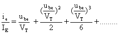
If the input signal is given as 'x' (where 'x' can be f.ex. sin(wt)), then the output 'y' will be :
![]()
And 'x' is a relative parameter which must always obey /x/<1 in order for the series to converge. If /x/<1 then it follows that /y/<1. The output current is 'ie' and the output parameter is then 'ie/Ie'. The input signal generating a current of 'ie' is 'uin', from the formula 'ie = uin*gm' It then follows from the transconductance formula that the input parameter we seek is 'uin/Vt'.
So, given the input 'x', defined as 'uin/Vt' and the output 'y, defined as 'ie/Ie', what does these things mean ?
If 'uin/Vt' exceeds 1, then the varying part of the current exceeds the Quiescent current Ie, and the stage is clipping. When the stage is clipping, our formula breaks down. If we are the find the distortion when the stage is clipping we'll have to resort to Fourier analysis.
To make this into a practical case:
Assume a transistor running at a current of 1mA. The gm is then 1/25 Siemens (The inverse of ohm, and the unit for transconductance, although also mhos is used (ohm reversed) ). An input signal of 1 mV will then generate an output current of 1/25 mA = 40 uA. But now note: This is the first order approximation. As can be seen from the series expansion above, we also have second and third order components. The first order coefficient should be pretty equal to 'gm', but what are the other two coefficients ?
The real equation relating input voltage to output current is : Ie = Is*exp((Ube/Vt)-1), called the Ebers-Moll equation. 'Is' is the 'leakage' current, but don't bother about it, we'll soon enough get rid of it. We are interested in finding the equation for the behavior around the quiescent point,. WE do this by adding small deviations 'ie' and 'ube' to the equation above. Resolving this, we get the much simpler equation: ie/Ie = exp(ube/Vt)-1, and its inverse: ube/Vt = ln(1+ie/Ie). These equations are called the signal equations, and will be used to get the coefficients for the series expansion above. We'll first make a series expansion of the first equation, and we will get:
We now introduce the efficiency parameter 'ni'. The point of introducing this parameter is to generate simpler formulas for calculating the distortion, and to gain a better understanding of how the distortion and other transistor parameters are coupled.
The parameter is defined as :
ni = ie/Ie
For a bipolar stage without local feedback, as the stage discussed above, ni is equivalent to ube/Vt, where we only consider the linear part of the series expansion. The equation above can then be written as:
![]()
The second order distortion is defined as the second order term divided by the first order term, and the third order distortion in the same manner:
2nd = ni/2
3rd = ni2/6
If the input signal is a sinusoid, then the following equations hold: (Ask me for proof, if you're interested tsandstr@online.no) where 2ndh is the second order harmonic distortion, and 3rdh is the third order harmonic distortion.
2ndh = 2nd/2
3rdh = 3rd/4
Putting it together:
2ndh = ni/4
3rdh = ni2/24
and remember, set ni = uin/Vt.
It is interesting to do the same exercise on FET transistors. The result is a simpler series, with only first and second order components. By inserting the efficiency parameter, one will get the following equation for the FET's 2nd harmonic distortion.
2ndh = ni/8
half the amount of the bipolar transistor. Some people have argued that the FET is a much more linear device than the bipolar. This equation shows this as only a partial truth, there is only a 6dB improvement.
It is well known that local series current feedback, (read - inserting an emitter resistor) reduces the distortion. The feedback factor can be written as:
D = 1 + gm*Re = 1 + (Ie*Re)/Vt
and the resulting efficiency/distortion equations is then :
2nd = ni/(2*D)
and
3rd = ni**2/(3*D)
or for the harmonic distortion:
2ndh = ni/(4*D)
3rdh = ni**2/(12*D)
Note that the efficiencyparameter ni is still defined as ie/Ie, but the input version is now ni = uin/Vth, where Vth = Vt*D.
There is a similar set of equations for the differential pair.
If the stage is completely in balance (which of course rarely happen), all second order components will be cancelled.
The no-feedback solution will have a basic transconductance of gm = Ie/(2Vt), which gives ni = uin/2VT
The corresponding distortion is then equal to the single stage, except for a mismatch parameter 'm' and a common mode signal factor 'c'
3rd = ni**2/3
and
2nd = (m+c)*ni/2
If the current source feeding the emitters have infinite output impedance, c approaches 0. The formula for c is c= ik/(2ie). More information on this in my AES Paper (WEB version coming soon). See the Single Stage Calculator
| Stage type | 2nd harmonic | 3rd harmonic |
| Bipolar single stage | ni/(4*D) | ni**2/(12*D) |
| FET Single stage | ni/(8*D) | Ideally zero |
| Bipolar differential stage | (m+c)*ni/(4*D) | ni**2/(12*D) |