Evolution of the Schematics
Also see the later schematics
The first design was taken directly from the paper by Otala and Lohstroh, AES 1973. To it was added a power supply only. The PCB layout and the mechanical design were done at EC.
Original Otala — first-series schematics
Only 10 amplifiers were made using these schematics. None exist today.
The next series was done after early 1976, and incorporated the first changes to the frequency compensation. The changes were made to improve the frequency response and slew rate of the amplifier.
Referring to the schematics above, the fixes were done on the first- and second-stage lead network (the RC’s between the emitters of the differential pairs); the lag networks on the collector sides were removed, and the input lag network was redimensioned.
After a breakdown of the first amplifier brought to the US, a non-intrusive (sound-wise) protection network was added to the amplifiers.
Several intermediate steps are missing, but at the end the design looked like what’s shown in the next schematics, which applies for amplifiers with serial numbers above 100 — these were heavily EC-modified. See the History section.
The real Electrocompaniet schematics, serial numbers approx. 100 and up
Note the reduced values of all input-stage resistors, indicating the increased quiescent current in these stages.
From serial no. 275, the Great Change was applied to the amplifiers.
This was the last of the EC designs, but in my own company I did two new modifications: one known only as the NRF Mod., the other known as “The Special Version”. The modifications were only further improvements, naturally following on from the EC time. See the NRF modifications page.
The “Special Version” schematic is shown here:
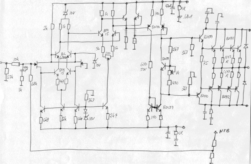
Note the heavily reduced values of the output-stage emitter resistors — down to 0.33 ohm from 1 ohm! This reduces the AB nonlinearity, as described in my 1982 AES paper.
Note also the changed input stage, with a JFET differential pair as a source follower. It was found that the bipolar input stage added distortion caused by its nonlinear input base current acting on the input resistors. (Which again shows: when we reduced the input resistors from 6k8 to 2k2, we heard a sound improvement and believed it was caused by improved frequency-response behavior above 20kHz — it may have been the 10dB distortion reduction that we heard!) To reduce this distortion further, the JFET pair was added. Further, a cascode pair was added to eliminate the Miller effect and the nonlinear voltage modulation of the critical first stage.
The gain distribution was also changed — the 3rd stage gain was increased by raising the load resistors from 2k2 to 3k3. More gain was needed to increase the overall feedback to 40dB. It was found that increasing this particular point (3rd stage) was the less critical of the options. However, we got slightly more relative modulation effect on the 3rd stage than we wished for.
All in all, approximately 100 amplifiers were modified, and an additional 50 Special Versions were made.
By the end of the ’80s and the beginning of the ’90s, I tried a few more changes to the amplifier design, which never made it beyond the lab bench. Only one amp exists with these modifications. They included emitter followers added before the 3rd stage, to reduce the modulation effect mentioned above.
Also see some of the later calculations made on this amplifier.
What about some thoughts on the “Perfect 25W” amplifier? Or the perfect preamplifier, which was realized, but …
Anything you find missing, or any comments, are appreciated — reach out via the about page.