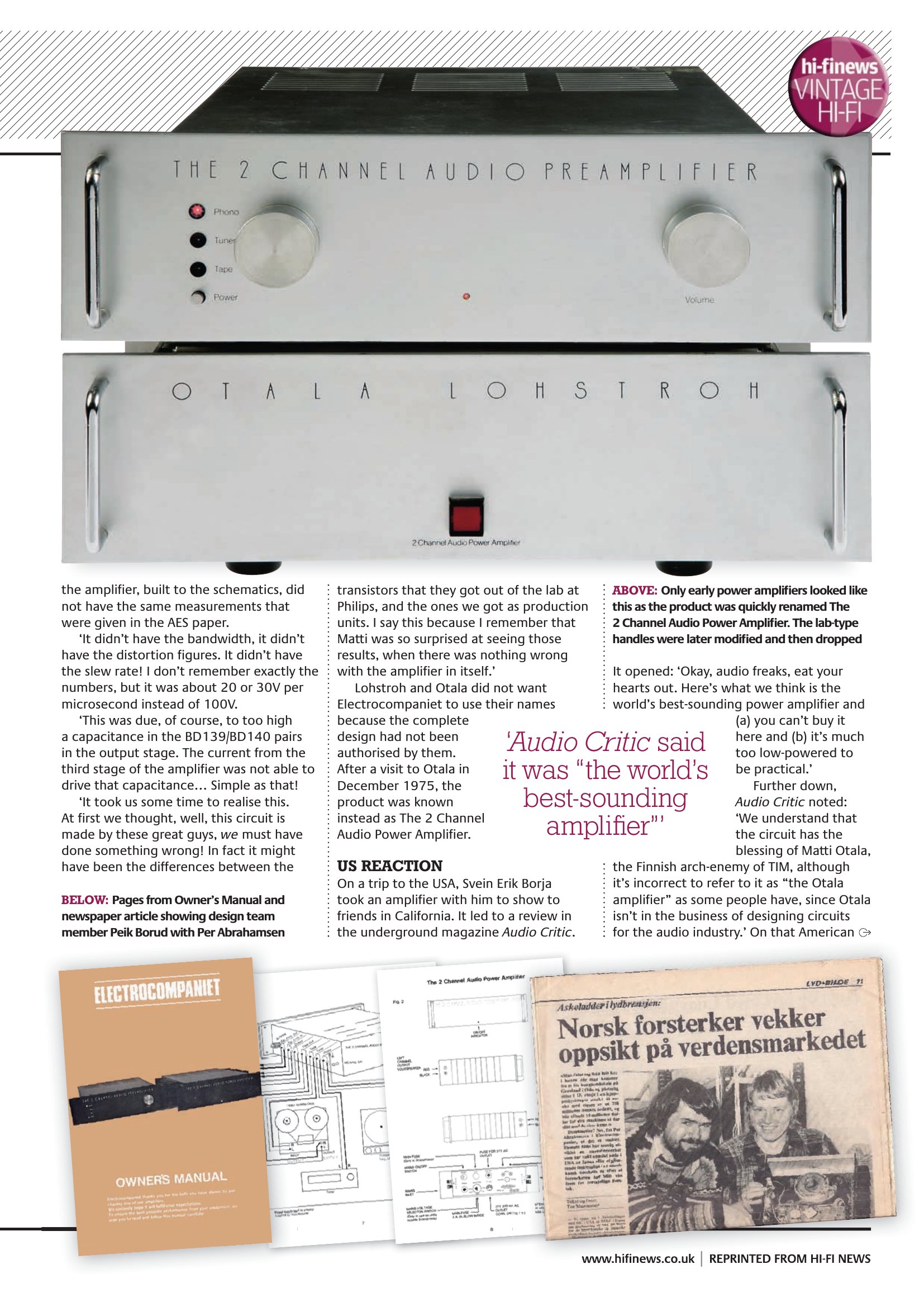
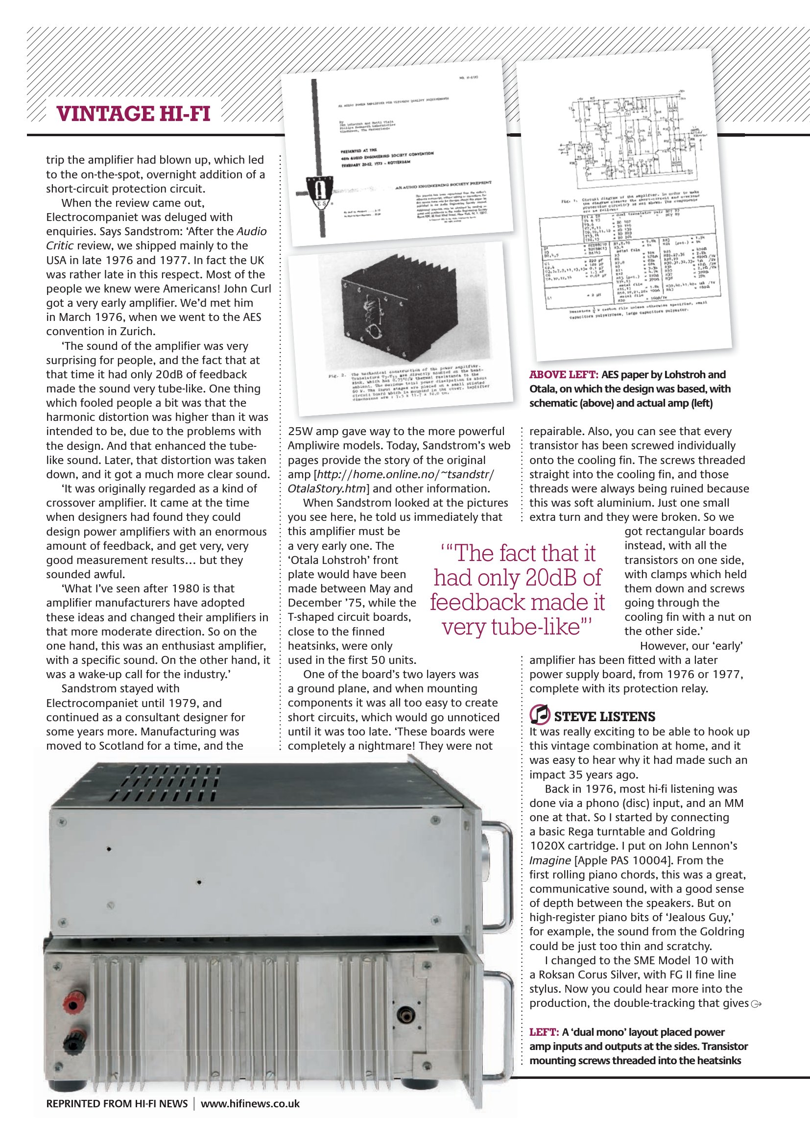
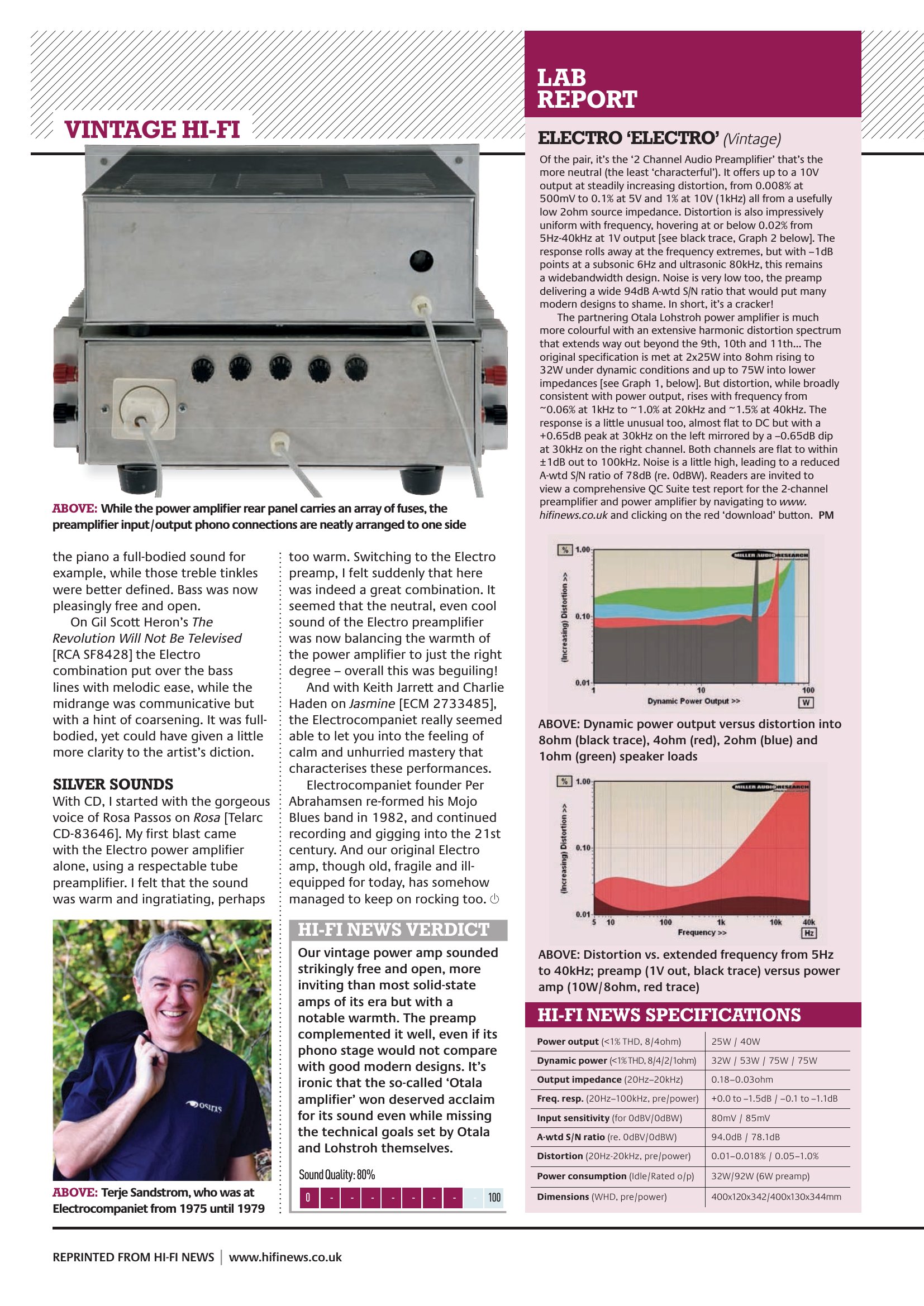
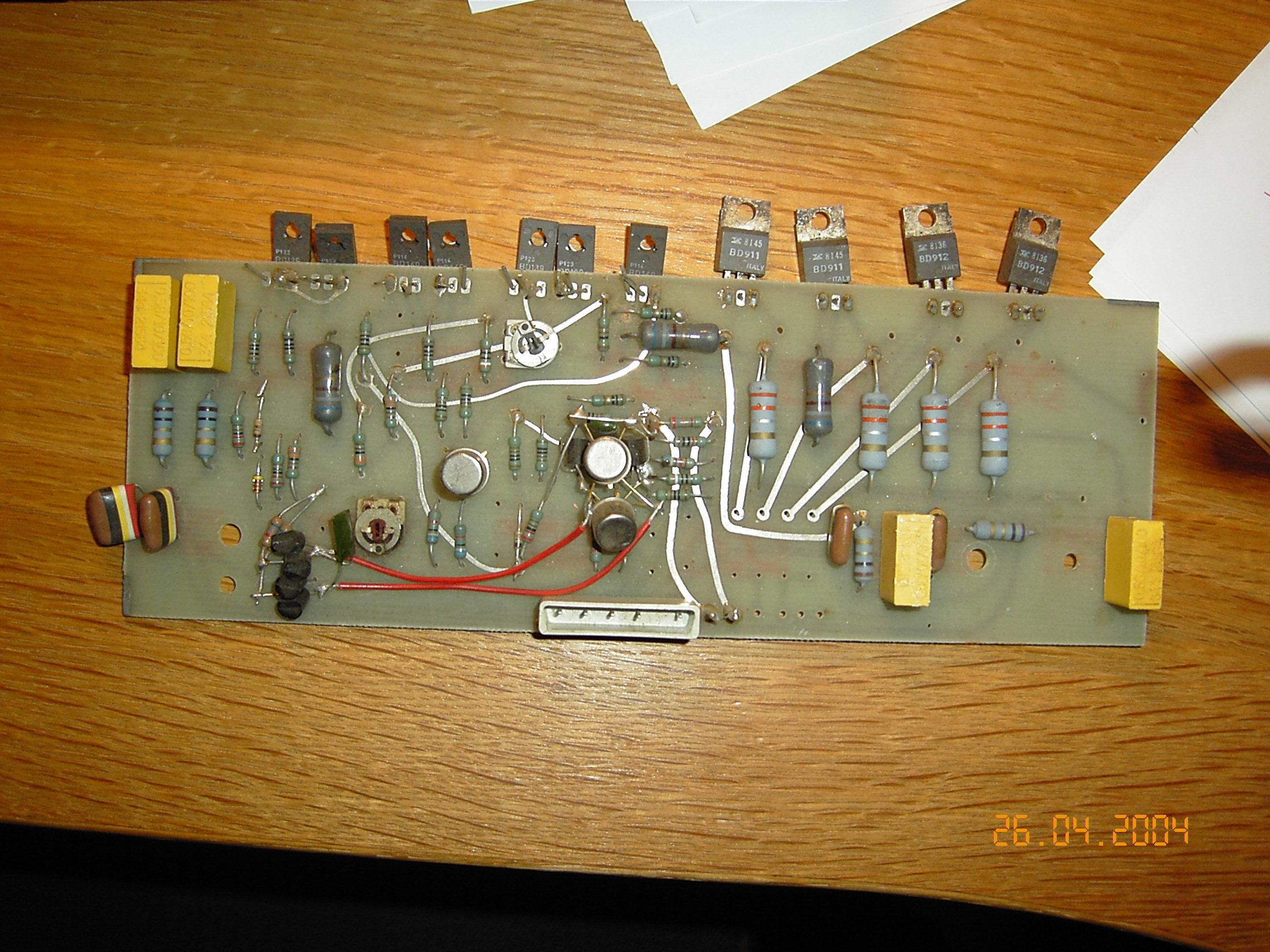
Welcome to the Terje Sandstrøm Audio Technology site
For several years I worked on the design of audio equipment for very high
fidelity use, primarily for Electrocompaniet. As I no longer work actively in
that field, I’ve put as much of what I know onto this site for anyone to look
at.
This site covers the audio technology I worked on, the history of the early
Electrocompaniet period from 1975 to 1980 and their “Otala” 25W amplifier, plus
schematics, troubleshooting guides, theory articles, my M.Sc thesis on weak
non-linearities, and other audio-design work.
My current work is in software development — see
my blog for that side of things.
Subsections of Hermit Audio
Chapter 10
History
The story of the early Electrocompaniet period (1975-1980) and the “Otala”
25W amplifier: the people involved, the press coverage, the brochures.
A story of the legendary 25W “Otala” amplifier as seen by Terje Sandstrøm, one
of the original designers.
Also see “The People Involved”, for other designers and
people who contributed.
Introduction — the birth of the Otala amplifier
At an AES conference in 1973, Dr. Matti Otala presented a paper describing the design of a TIM-free audio amplifier. Among those attending was Svein Erik Børja, a Norwegian record and broadcasting producer and dedicated audio enthusiast. Børja was widely recognised for his exceptional listening ability—what audiophiles of the day referred to as a “Golden Ear.” Dissatisfied with the sound quality of many transistor amplifiers of the time, he immediately recognised the significance of Otala’s work. The theory behind TIM also provided an explanation for imperfections that he himself had consistently identified by listening.
Looking back, this became one of the foundations of our design philosophy: careful listening, objective measurements, and theoretical analysis. All three had to point in the same direction before we considered a design change to be successful.
Børja brought the paper to Nils Jørgen Kjærnet at Nera in Oslo. Together they built two prototype amplifiers based on the Otala/Lohstroh schematics. Kjærnet designed the printed circuit boards and, to the best of my knowledge, also contributed to the mechanical design.
The promising results led Børja to contact his friend Per Abrahamsen, who was then running Electrocompaniet. Per decided to build a couple of amplifiers to evaluate the design. They fulfilled all expectations and sounded so good that Electrocompaniet decided to manufacture a production series, marking the company’s transition from professional audio equipment to high-end audio.
I started hanging around Electrocompaniet in the autumn of 1974 and began working for Per in the spring of 1975. One of my first tasks was assembling the first production series of the Otala amplifiers—a run of ten units built on the same printed circuit boards as the original two prototypes.
During the summer I started looking at the design. Having designed and built electronic equipment as a hobby since my early teens, I naturally wanted to understand how it worked. At that time neither Per nor I had much experience in high-end audio design. In retrospect, that may well have contributed to the amplifier’s success. We didn’t know how it was supposed to be done, so we worked it out ourselves within the framework provided by Otala’s design.
In many ways we belonged to the first generation of amplifier designers to develop products with TIM as a primary design criterion. We were learning as we went, building on the foundation laid by Otala’s work.
The first Otala amplifier in “production”
The first amplifier series used the same printed circuit boards as the first
two prototypes. The PCB was a two-layer design — we called it a T-board, due to
its shape. The power transistors were mounted onto the cooling fin from both
sides of the stem of the “T”. One layer of the board was a ground plane (Nera
being an RF company, that wasn’t so strange). The ground plane caused us a lot
of mounting problems, because the component legs often got stripped when they
were squeezed through the holes in the PCB, causing small metal pieces from the
legs to curl up and make sweet, nearly invisible, shorts to the ground plane.
We did see smoke …
In the autumn of ‘75 we started to get some attention, and a visit to Matti
Otala at the VTT (Valtion Teknillinen Tutkimuskeskus — the Technical Research
Centre of Finland), where he worked as a professor, became necessary. There
were several reasons:
We had named the amplifier “Otala-Lohstroh” after its inventors, and Otala
wanted to see the amplifier before he and Lohstroh could possibly allow us to
use his name.
At the same time, we started to experience problems with the amplifier — it
didn’t quite meet the specifications stated in the AES paper. We needed his
help.
As it turned out, the amplifier was renamed to “The 2-channel audio power
amplifier”, which was the name used for the rest of the amplifier’s lifetime.
The relationship with Otala was established, and he visited the company on
several occasions. There is still good contact between Otala and
Electrocompaniet.
Period of confusion, start of revision
It was early 1976. We started to invest in measuring equipment. The company
slowly turned into an audio amplifier company. It lost several of its old
customers; the loudspeakers it sold became more neglected. We worked from
early morning into the late nights. That would be the standard for the next
4 years. An amplifier brought to the US by Svein Erik blew
up at the first listening test — embarrassing. We used the night to invent a
new type of short-circuit protection. We didn’t want
anything that could affect the sound, so we simply used a high-impedance
circuit to sense the current through the output transistors, and then used a
relay to switch off the voltage to the output transistors. It worked!
We now understood that we had to start changing the amplifier. Svein Erik’s
golden ears became even more important than ever before. We were in uncharted
territory; the old measurement methods could not be trusted. We had to rely on
our own methods, our own interpretations of the measurement results. Now began
an active period of theory, practice, and reading articles (Svein Erik provided
us with articles en masse, on all aspects of audio design and electronics
design in general).
We found that the compensation scheme used in the amplifier did not work
correctly. As we measured the bandwidth to be far less than specified, we
needed to redesign these filters. The amplifier used shunt feedback — one of
its really strong points — with an input lag compensation; at each of the
three amplifying stages, a lead-lag compensation was introduced. These did not
match the actual poles we measured. One of the reasons for this, we assumed,
was that the original design used “fresh,” newly developed Philips
transistors. As both Otala and Lohstroh were working at the Philips labs in
Eindhoven at the time of the design, we assumed they had access to better
transistors. (I don’t remember if Otala ever confirmed this to be the case.)
In any case, a period followed where we changed the compensation back and
forth with little or no effect. We did achieve something, but no significant
improvement.
We had also now measured the distortion (having just bought our first
distortion measurement set and spectrum analyzer). It wasn’t pretty — the
distortion was far worse than specified, and performance was far below even
our own expectations. Again we didn’t manage to do anything significant at
first.
A major change came first when we started to change the quiescent current of
the transistors. The design was in fact done as a mix between the old way and
the new way. Older design books teach that you should use low current in the
first stage due to noise. This was also done here (see “Noise Optimisation”
for an explanation of why that’s not actually the case). We knew this theory
was wrong, so we increased the quiescent currents, which decreased the
resistance and again dramatically increased the bandwidth of the amplifier.
The distortion also went down — not dramatically, but enough to make a
significant change for the better in the sound (see “Transistors, Resistors,
Current and Distortion” — not yet written).
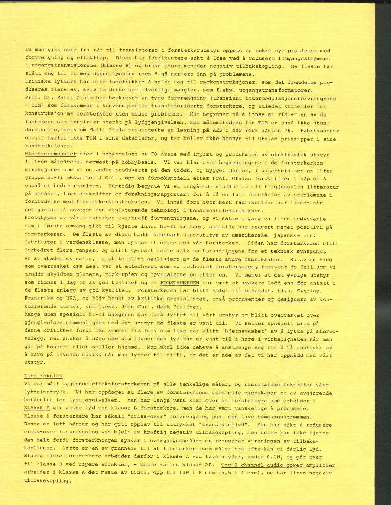
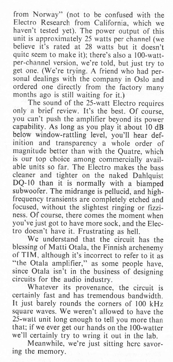
The Audio Critic
At this time we started to hear rumours about a
test in
the US on our amplifier. One day our mail started to overflow, and a few days
later we got hold of the test ourselves. It was in a magazine named The Audio
Critic, and the test was fabulous. It started:
Audio freaks - Eat your hearts out: This is the worlds best sounding
amplifier, and One: You can’t buy one in this country (The USA!), and Two:
(not surprisingly - the only slightly negative in the whole test) It is too
low powered to be counted.
Suddenly we had more requests for amplifiers than we could hope to handle.
Sales boomed. It was mid-‘76.
We worked throughout the summer, from morning until late at night, seven days a week. It was an intense period, driven by enthusiasm and the determination to make the amplifier a reality.
The great change
Dr. Otala’s work on TIM was often interpreted as an attack on high-feedback amplifiers. While it is true that high-feedback designs can be more prone to TIM than low-feedback designs, there is nothing inherently magical about low feedback.
The primary goal of any amplifier is to reproduce the input signal as accurately as possible, neither adding nor subtracting anything. TIM is simply one form of distortion; reducing one type of distortion at the expense of increasing another is not, in itself, an improvement.
It is true that some types of distortion are more objectionable to the ear than others, so there is always a balance to be struck. If, for example, 0.1% TIM is considered subjectively equivalent to 1% THD, then an amplifier with 2% THD and 0.07% TIM is likely to sound worse than one with 1% THD and 0.1% TIM.
We gradually came to realise that achieving the right balance between different forms of distortion was the key. It was not simply a matter of balancing THD against TIM, but also low-frequency distortion against high-frequency distortion, frequency and phase response against nonlinear distortion in general, and so on.
This insight led to The Great Change.
One night (it always seemed to happen at night!) we increased the feedback by 10 dB, bringing the total feedback to 30 dB. The improvement in sound quality was remarkable—and completely contrary to the prevailing beliefs within our own community.
From that point on, only minor adjustments were made to the amplifier. It had essentially reached the form it would retain throughout the rest of its life at Electrocompaniet.
Although never a high-volume product, the amplifier earned an international reputation and became the foundation on which Electrocompaniet built its name.
On marketing
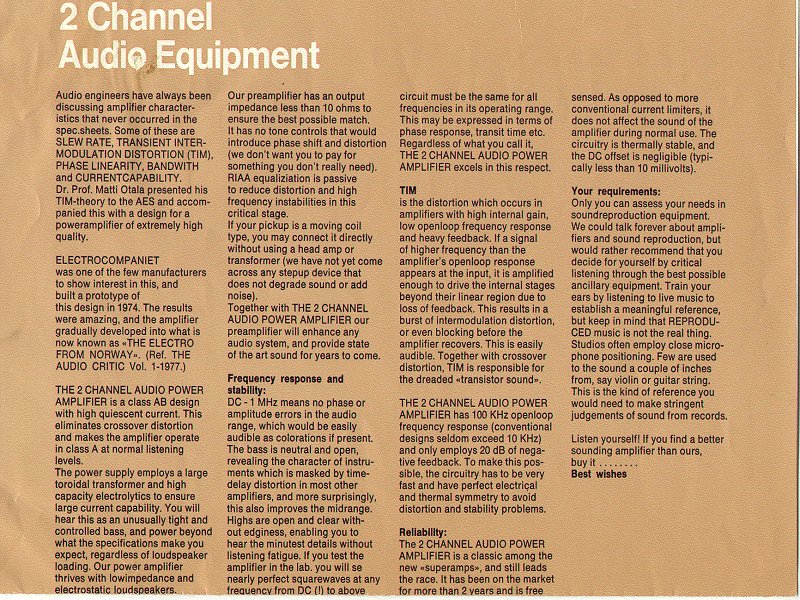
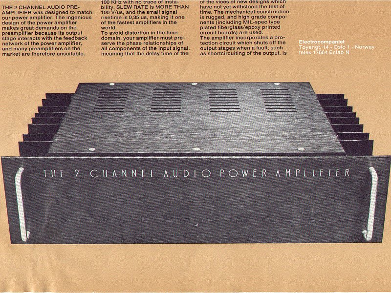
We did brochures! The first one was rather
technical. The second one was more
professional. The rest of the marketing was done by word-of-mouth. The fact
that the amplifier and the company were both hard to get hold of stimulated
the market. Here was a mysterious company with a killer amplifier. Audio
people love such stuff!
See the evolution notes, handwritten in Norwegian, but with English text extracted.
Subsections of The Story of the "Otala" Amplifier
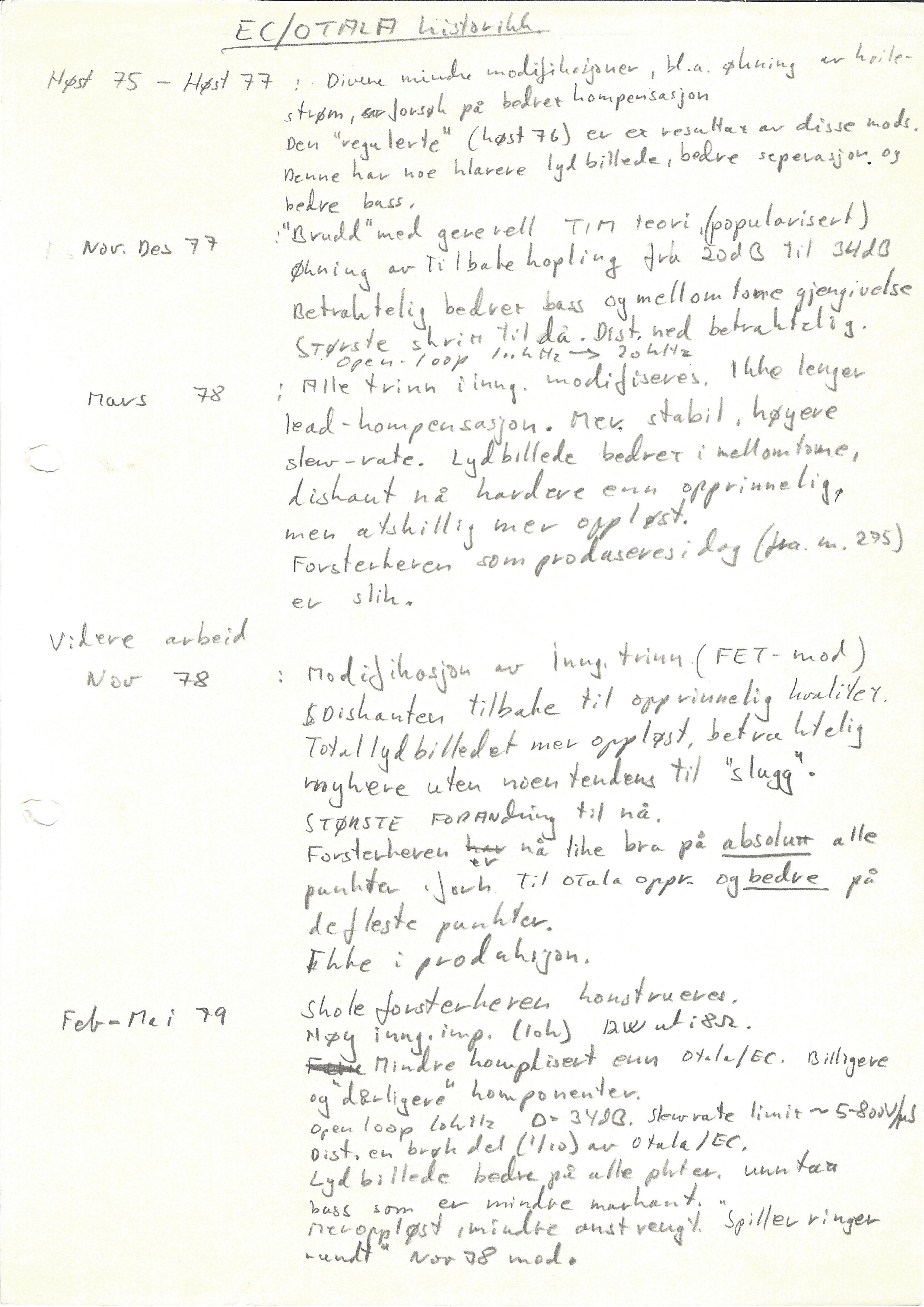
The Evolution of the Otala/EC Amplifier — Handwritten Notes
EC/Otala historikk
I have found an older handwritten page about what was changed when, which can be useful to see the evolution of the amplifer, probably written around 1980. It is course, very honest some places, but we can live with that. And I see it is my own handwriting. The image of the note is in Norwegian, but the extracted text is in English.
English Translation
Autumn 75 – Autumn 77
Various minor modifications, among them increased idle
current, attempts at improved compensation.
The “regulated” version (Autumn 76) is a result of these mods.
This one has a somewhat clearer sound image, better separation and
better bass.
Nov. Dec. 77
“Break” with the general TIM theory (popularized).
Increase of feedback from 20 dB to 34 dB.
Considerably better bass and midrange reproduction.
Biggest step so far. Distortion down considerably.
Open loop 100 kHz → 20 kHz.
March 78
All stages, incl. input, modified. No longer
lead compensation. More stable, higher
slew rate. Sound image better in the midrange.
Treble now harder than originally,
but considerably more resolved.
The amplifier being produced today (from no. 295)
is like this.
Further Work
Nov. 78
Modification of input stage (FET mod).
Treble back to original quality.
Overall sound image more resolved, considerably
softer without any tendency toward “slagging.”
Biggest change so far.
The amplifier is now just as good in absolutely every
respect, compared with the original Otala version, and better in
most respects.
Not in production.
Feb.–May 79
The school amplifier designed.
High input impedance (10 kΩ), 12 W output into 8 Ω.
Less complicated than Otala/EC. Cheaper
and poorer components.
Open-loop bandwidth 20 kHz, feedback 34 dB. Slew-rate limit ~5–800 V/µs.
Distortion a fraction (1/10) of Otala/EC.
Sound image better in every respect, except
bass which is less pronounced,
more resolved, less strained. Runs rings
around the Nov. 78 mod.
Norwegian Transcribing
Høst 75 – Høst 77
Diverse mindre modifikasjoner, bl.a. økning av hvile-
strøm, forsøk på bedret kompensasjon.
Den “regulerte” (høst 76) er et resultat av disse mods.
Denne har noe klarere lydbilde, bedre seperasjon og
bedre bass.
Nov. Des 77
“Brudd” med generell TIM teori (popularisert)
Økning av tilbakekopling fra 20 dB til 34 dB.
Betraktelig bedre bass og mellomtone gjengivelse.
Største skritt til da. Distortion ned betraktelig.
Open loop 100 kHz → 20 kHz.
Mars 78
Alle trinn inng. modifiseres. Ikke lenger
lead-kompensasjon. Mer stabil, høyere
slew-rate. Lydbildet bedre i mellomtone.
Diskant nå hardere enn opprinnelig,
men adskillig mer oppløst.
Forsterkeren som produseres i dag (fra nr. 295)
er slik.
Videre arbeid
Nov 78
Modifikasjon av inng. trinn (FET-mod).
Diskanten tilbake til opprinnelig kvalitet.
Total lydbildet mer oppløst, betraktelig
mykere uten noen tendens til «slagg».
Største forandring til nå.
Forsterkeren er nå like bra på absolutt alle
punkter, i forhold til Otala opprinnelig og bedre på
de fleste punkter.
Ikke i produksjon.
Feb–Mai 79
Skoleforsterkeren konstrueres.
Høy inng. imp. (10 kOhm) 12W ut i 8 Ω.
Mindre komplisert enn Otala/EC. Billigere
og dårligere komponenter.
Open loop båndbredde 20 kHz, feedback 34 dB. Slew-rate limit ~5–800 V/µs.
Distortion en brøkdel (1/10) av Otala/EC.
Lydbilde bedre på alle punkter, unntatt
bass som er mindre markant,
mer oppløst, mindre anstrengt. Spiller ringer
rundt nov 78 mod.
The People Involved
Several people were involved in the development of the 25W amplifier. This
chapter takes the history from the perspective of the people involved, in
chronological order.
A Finnish professor named Matti Otala
(also here). On sabbatical at Philips in Eindhoven,
together with Jan Lohstroh he designed a TIM-free amplifier. It was one
step in Otala’s quest against the new distortion called TIM, and later DIM.
Svein Erik Børja, a Norwegian broadcast and record producer, heard the
presentation given by Dr. Matti Otala at an AES conference in Copenhagen in
1973. Together with Nils Jørgen Kjærnet at Nera he built two (or five) units based on the Otala/Lohstroh schematics.
Per Abrahamsen was contacted by Svein Erik, who knew him from his Mojo
Blues days as a producer, and also knew that Per had an audio/electronics company. Per was
mostly working with PA equipment, but the arrival of the Otala amp turned his
company, Electrocompaniet, into an audio company.
At this time several others were involved with the company, but I don’t
remember all of them, mostly because they were before my time, and also
because they slowly disappeared as the company changed from a PA company to an
audio company. Among these were Petter Hjerpseth and Klaus Væthe Jr.
The latter later became a good friend of mine, and we tried to make an audio
company together in 1983, with the help of Paal Rasmussen, my former
partner at NRF — more on that later. Petter
disappeared during 1975; Klaus stuck with the company on and off until
sometime in 1977/78.
I (Terje Sandstrøm) first turned up in late 1974, and started to visit EC
on a monthly basis. After half a year of this, Per told me we were both better
off if I started to work for him, instead of just spending his time. In the
beginning I mostly did assembly work, but during 1975 I worked myself up the
ladder, and later I did more and more of the theoretical work on the
amplifier, calculations and so forth. I stayed until 1979, but did some part
time work and consulting for EC until 1982.
It is important to note that Svein Erik stayed with the company as its Golden
Ear for a very long time. In a way this was his hobby!
Peik Borud entered the company in 1976. He was an M.Sc. engineer in
electronics, and an audio freak. He stayed throughout 1978, and was, together
with Per and me, one of the basic designers of the 25W amplifier in this
period. Peik did a lot during his time at EC.
Paal Rasmussen entered the company in 1977 and stayed on and off for
slightly less than a year. He came from Seas AS, a loudspeaker company, and
before that he had worked in England with several of the famous designers
there. He and I were two of the three who started The Norwegian Radio
Manufacturing Company in 1979 — more on this later.
Kjell Winther was our record provider, and got amplifiers in return. He
was also a hi-fi nut, working in a record store, and provided us with the
latest and best-sounding records for our sound tests.
Nils Kvam was a record producer who also worked with listening tests and
also provided opportunities for the company sales-wise. He stayed way longer than me.
Øistein Klevhus helped me with the Engineering High School (I was rarely
present …), and I got him a part-time job at EC from early ‘78 (or late ‘77)
until spring ‘79. We did the School Amplifier together,
spring ‘79.
Two of the people in production who really stayed for a while were Knut Arne
Jacobsen and his then-girlfriend Aud. There were also a couple of girls
who came from Tandberg to work in production — (their names are not
remembered). These also stayed for quite a while.
There were also some sales and managing people (Helge …, Jan
Richter, among others) involved from period to period. I’m working on
re-remembering their names. Any help from others is appreciated.
Others who contributed included, for example, Svein Erik’s brother, Bjørn
Børja, from Seas AS, who designed a cute little moving-coil amplifier that EC
manufactured for some time.
During 1979 the company relocated, I gradually left, and new people joined. Unfortunately, I no longer remember all of their names.
The first era of the original Otala amplifier came to an end around 1979–1980, marking the beginning of a new chapter for Electrocompaniet. The company moved to Skårer, where it remained until its bankruptcy in 2004. It was then acquired by Westcontrol and relocated to Tau in Rogaland.
Per continued with Abrahamsen Audio, where he reintroduced the Two Channel Audio Amplifier. However, I am not familiar with the technical details of that version.
This text was originally written some time in the late 1990’s, and minor
updates around 2005 and 2026
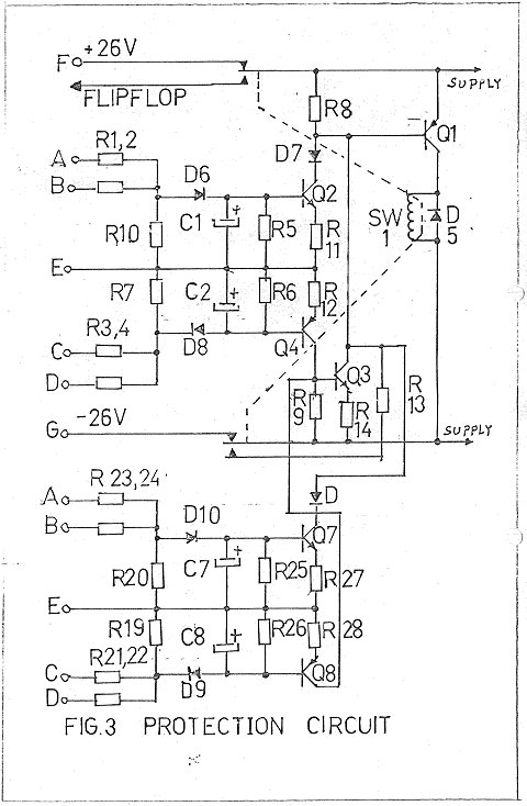
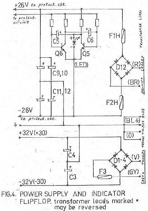
Protection Networks
Protection networks, power supplies, and other stuff not so interesting, but
still needed.
You’ve read the section on how this came about? If not,
go back and do so! Otherwise, take a look
at the world’s first protection network that did not affect the sound AT ALL.
Yes — it is the first one!
The design is very simple: passive sensing of current, then triggering a relay
which removes the supply voltage from the output stage. As you probably know,
the EC design uses one power supply for the voltage-amplifying stages and one
for the power output, where all the large currents go. This separation made
this protection scheme work. If not, big bangs would be heard …
The power supply also needed some care.
However, we did not make it difficult. The major point here was the use of
small capacitors instead of the sluggish big ones everybody else used at that
time. We understood that small capacitors in parallel were a better choice
than single big ones.
The cabling was another issue — more on that later.
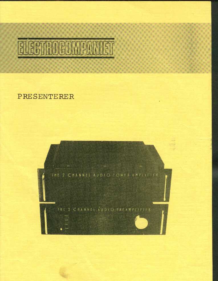
Marketing Brochures
We did brochures! See the Otala story for the
context.
Our first brochure
It was rather technical.
The two remaining pages are still waiting to be scanned.
Our second brochure
More professional this time :-)
Norsk Radiofabrikk
Norsk Radiofabrikk — The Norwegian Radio Manufacturing Company
The company was founded in 1979 by Espen Evensberget, Paal Rasmussen, and myself. We aimed to develop and market our own designs, but most of our work involved modifying and refining the Two Channel Audio Amplifier.
The company also put out its own press release, “Tre Faser i en Utvikling”
(“Three Phases in a Development”), about the story of the Otala power
amplifier including the NRF modifications, written in 1979 — that document
hasn’t survived, or hasn’t been found again yet.
Third-party coverage of the early Electrocompaniet amplifiers and Norsk Radiofabrikk
This page collects historical third-party coverage of the early Electrocompaniet amplifiers and Norsk Radiofabrikk, including links to magazine articles, as well as other people’s articles, blogs, and websites that are worth reading.
Where original online sources could not be found, scanned copies of historical magazine and newspaper articles have been included to help preserve this material. Permission has been requested from the copyright holders where possible.
Press coverage of the early Electrocompaniet “Otala” amplifier.
Articles
These are copies of magazine articles, as they have not been found online.
In some cases you can download issues, and links to that are in each underlying page.
Links to articles which relates to the history, including blog posts, and some interesting other related audio stuff
Tracking Angle, by Jan Omdahl, 2023 How a Small Norwegian Hi-fi Brand Ended Up With Credits on Michael Jackson’s Album Covers, includes the early start up story.
The links here require a subscription for Aftenposten, A-Magasinet is a part of Aftenposten. The article is in Norwegian.
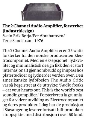
The Norwegian “A-Magasinet” had an article March 3rd 2017about the 100 best Norwegian designs, judged by a brioad expert jury, with designs ranging from 1920 to 2014, nearly 100 years, and among them “The 2 Channel Audio Amplifier.
Subsections of Early Electrocompaniet — Press & Links
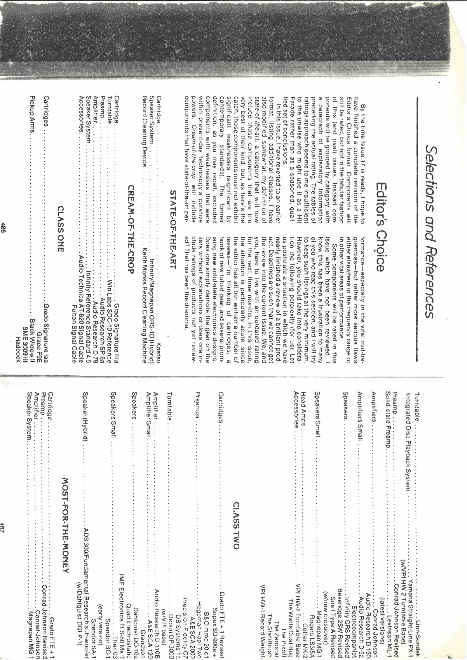
The Absolute Sound (1979)
This is an extract from The Absolute Sound, Issue 16, 1979. The amplifier is listed as a recommended amplifier on the reference list.
The copies of this is mangled, and the first page of the review is missing, but the rest is there.
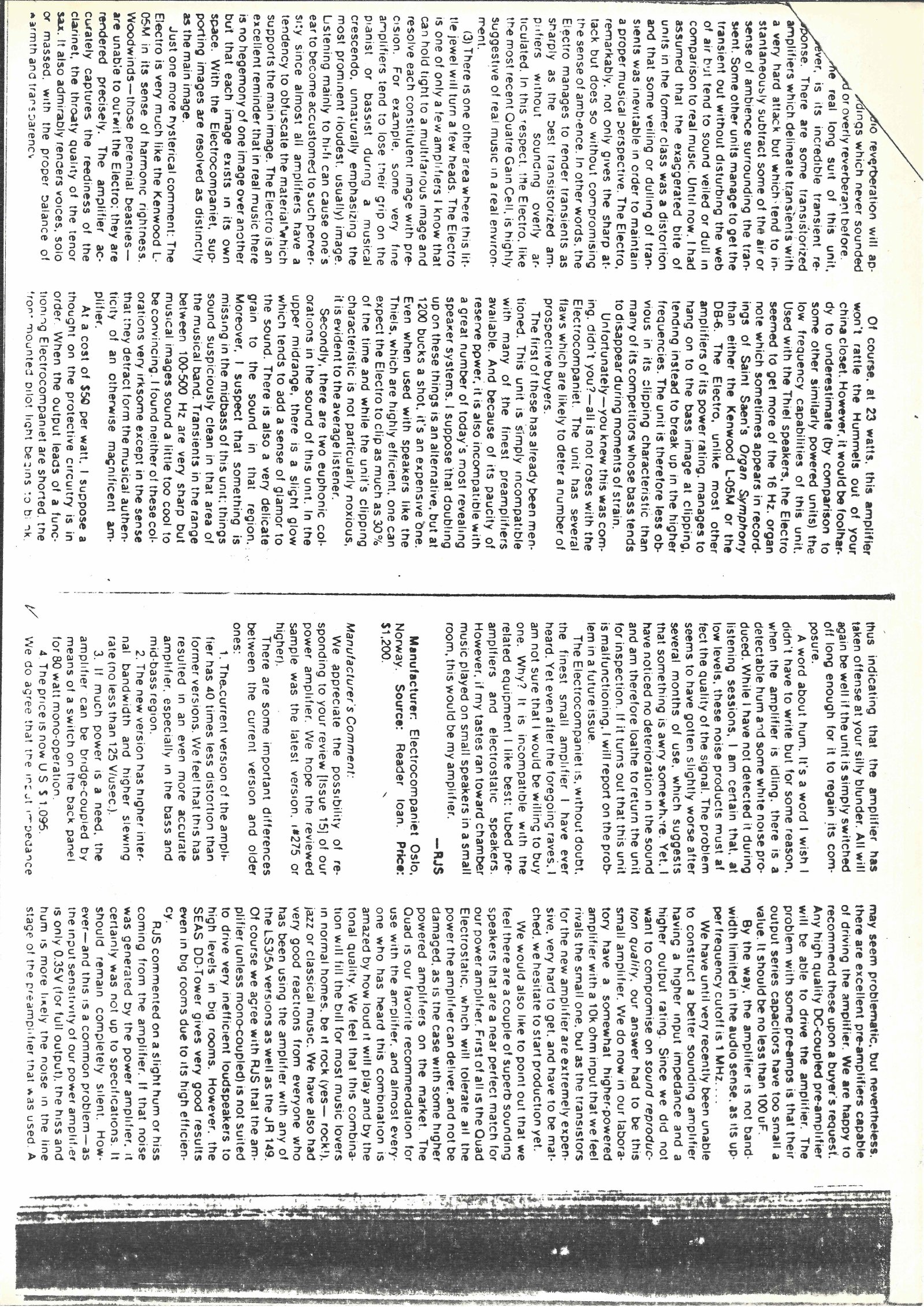
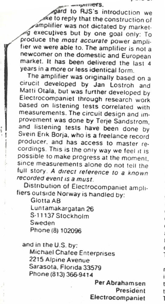
The Audio Critic (1976-77)
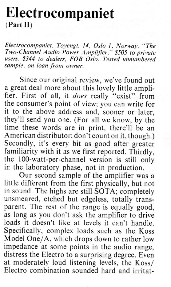
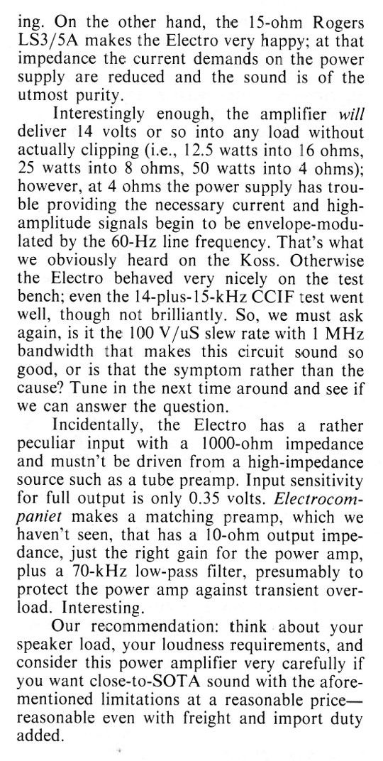
The Audio Critic tests, including the “Okey, audio freaks, eat your hearts out. Here’s what we think is the world’s best-sounding power amplifier”, which triggered the international fame of the amplifier and company. This was the real start!
If you want, you can download the older issues of The Audio Critic here, and below I state in which year and edition.
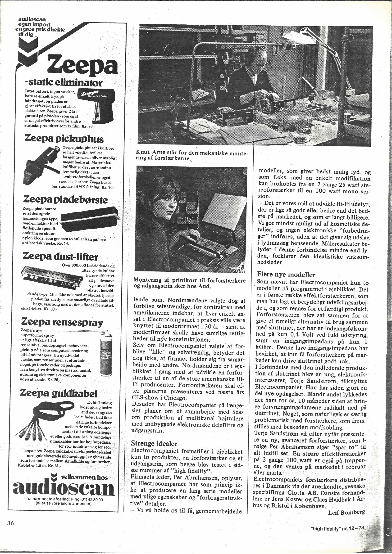
“Norsk idealisme bag ny forstærkerserie” (“Norwegian idealism behind new
amplifier series”) — a profile of Electrocompaniet in the Danish magazine
high fidelity, issue 12, 1978, pages 35-36. Covers the company’s origins,
Per Abrahamsen, Svein Erik Børja’s introduction to Matti Otala’s work, and
the early production process, with Terje Sandstrøm (then the company’s
udviklingsingeniør — development engineer) pictured working on a prototype.
By Leif Bomberg.
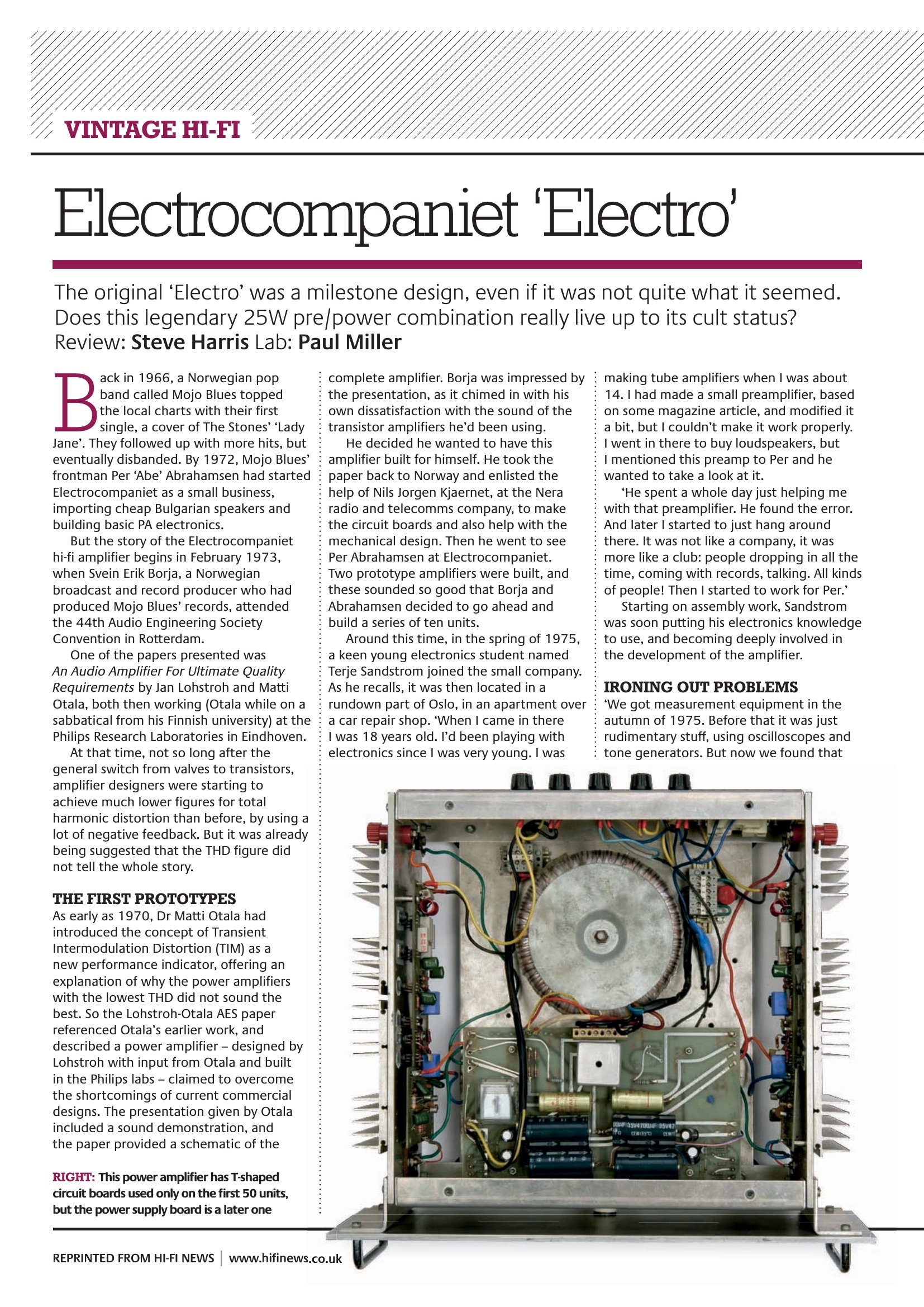
Hi-Fi News: "Electrocompaniet 'Electro'" (2012)
“Electrocompaniet ‘Electro’” — a Vintage Hi-Fi retrospective review and lab
report on the original 25W “Otala” pre/power combination, published in
Hi-Fi News, January 2012. Review by Steve Harris, lab report by Paul
Miller, including an interview with Terje Sandstrøm about the amplifier’s
early history and the Audio Critic review — see
the Otala story for the same events from the
designer’s side.
Other Norwegian press articles
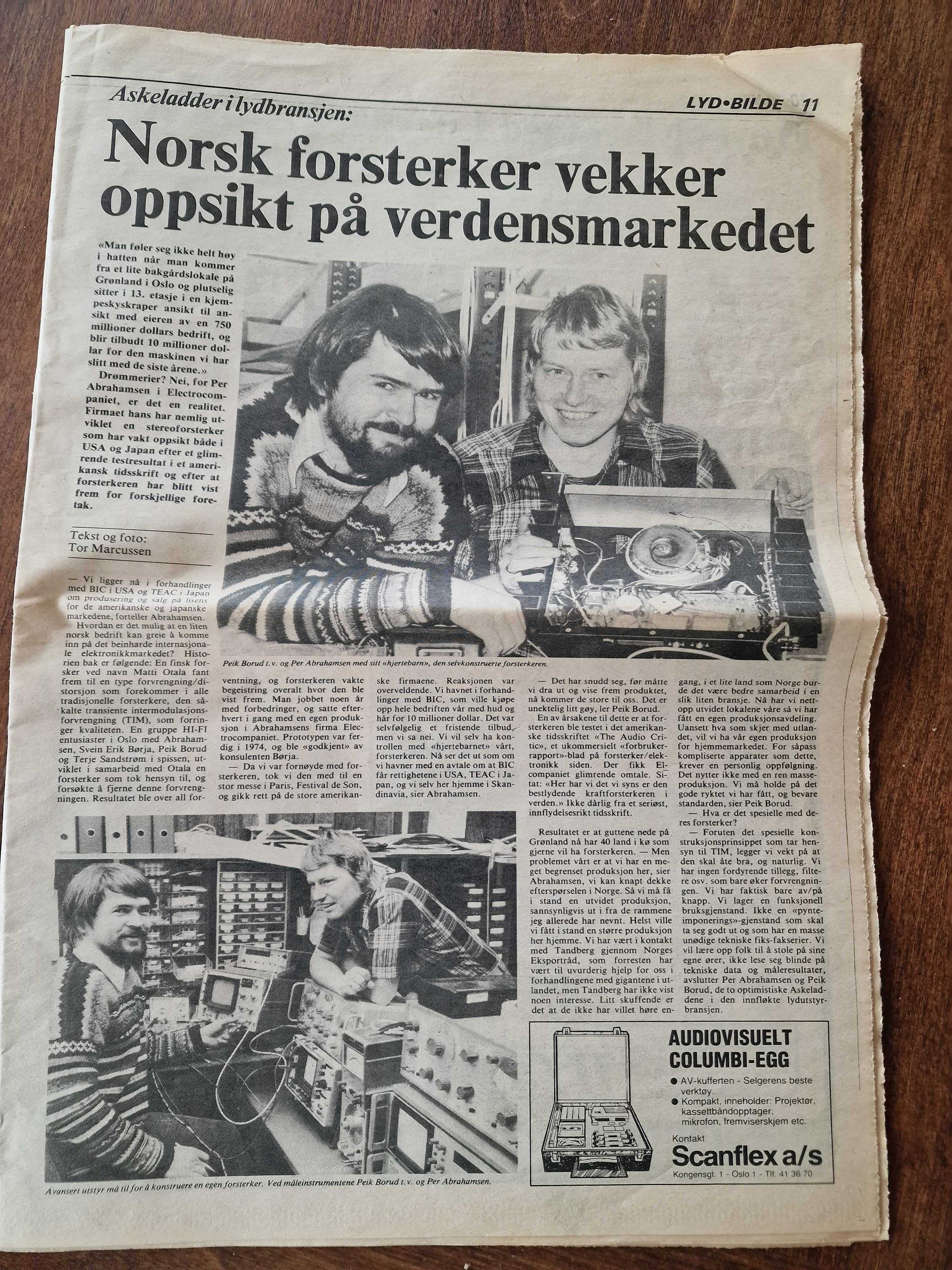
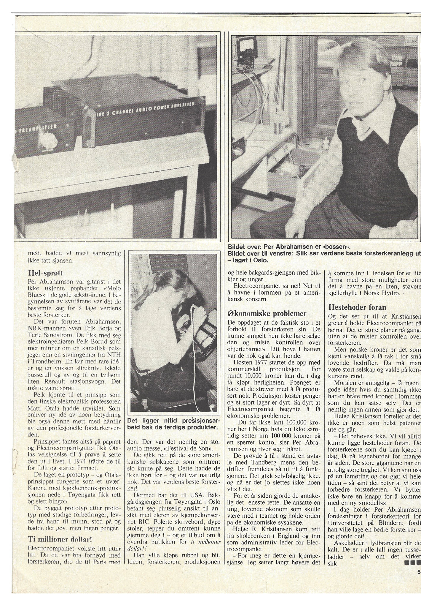
A series of Norwegian press articles from 1976 to 1978, from many different Norwegian magazines and papers.
They are not technical, some are from daily papers and some are from popular ordinary magazines.
HiFi Nytt - Norsk Ukeblad, nr 34 1977
Lyd Og Bilde nr 39, 24/9-2/10, 1977
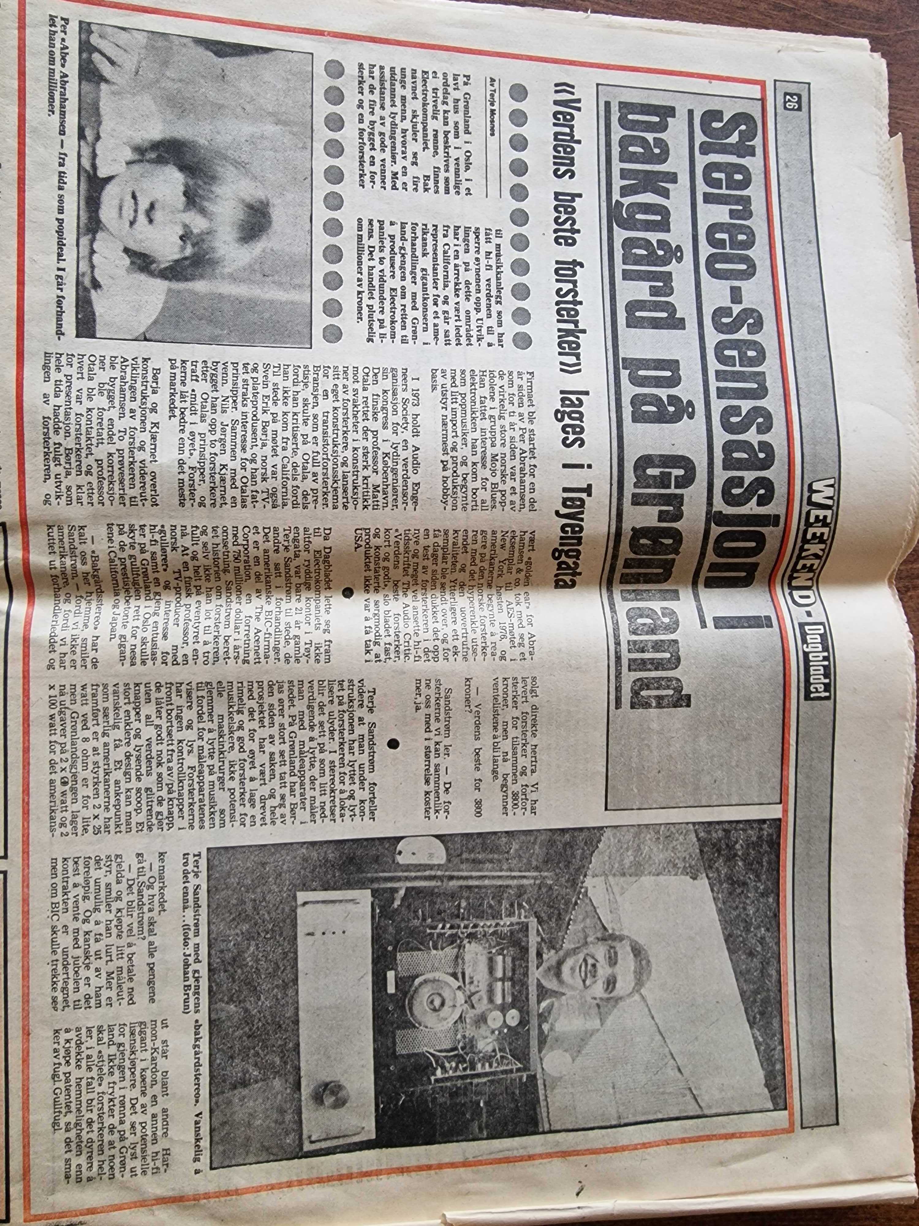
Dagbladet Weekend 27. Mai 1977
Express #12/13 1979
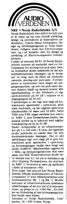
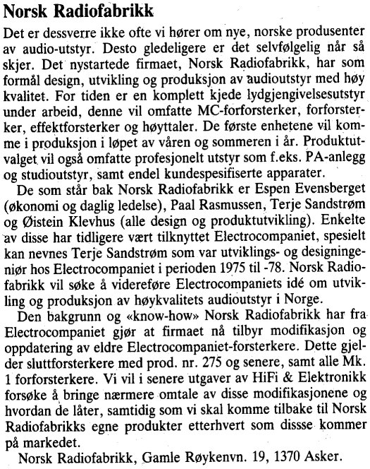
Norsk Radio Fabrikk
Norsk Radio Fabrikk — Press Coverage, 1980/81
Press coverage of Norsk Radiofabrikk and its modified Electrocompaniet
amplifiers — see the History section for the
story of the company itself.
Danish High Fidelity no. 2, 1981
Hi-Fi & Elektronikk no. 2, 1980
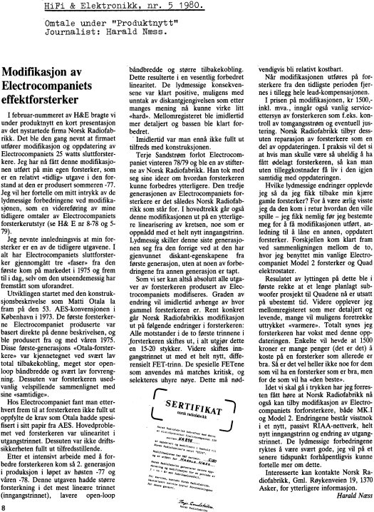
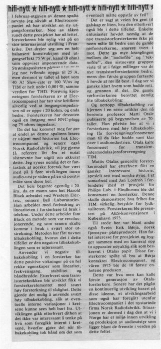
Hi-Fi & Elektronikk no. 5, 1980
Musikkavisen PULS no. 2, 1980
Musikkavisen PULS no. 4, 1980
External links
Other people’s articles and sites worth a read.
(none added yet)
Chapter 20
Technical Reference
Technical Reference
Schematics, troubleshooting guides, and calculations for the Electrocompaniet
amplifiers — the true EC factory designs, plus what came after: my own
NRF-era (Norsk Radiofabrikk) modifications and personal work, kept clearly
separate below.
See Post-EC / NRF for what came after — not EC factory work,
my own modifications and designs from the NRF era (1979 onward), kept
separate in the menu on the left.
Not ported: distortion_calculators.htm and SingleCalc.htm (an ActiveX
distortion-calculator control — only ever worked in old IE, and the control
binary itself isn’t something to carry forward) and a_strange_one.htm
(linked from the old site as “a further schematic variant”, but the actual
page content is just a generic “site under reconstruction” placeholder — no
real schematic survives there).
One gap filled in during migration: the old site’s schematics page said
“SCHEMATIC 5 is coming later” for the Special Version schematic and never
delivered it, but the scanned image existed unlinked in the old site’s
files — it’s now included on the NRF modifications page.
The first design was taken directly from the paper by Otala and Lohstroh, AES
1973. To it was added a power supply only. The PCB layout and the mechanical
design were done at EC.
Only 10 amplifiers were made using these schematics. None exist today.
The next series was done after early 1976, and incorporated the first changes
to the frequency compensation. The changes were made to improve the frequency
response and slew rate of the amplifier.
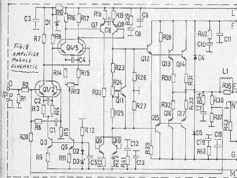
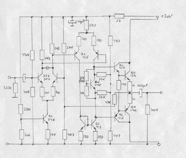
Referring to the schematics above, the fixes were done on the first- and
second-stage lead network (the RC’s between the emitters of the differential
pairs); the lag networks on the collector sides were removed, and the input
lag network was redimensioned.
After a breakdown of the first amplifier brought to the US, a non-intrusive
(sound-wise) protection network was added to
the amplifiers.
Several intermediate steps are missing, but at the end the design looked like
what’s shown in the next schematics, which applies for amplifiers with serial
numbers above 100 — these were heavily EC-modified. See the
History section.
Note the reduced values of all input-stage resistors, indicating the increased
quiescent current in these stages.
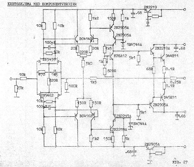
From serial no. 275, the Great Change was applied to the amplifiers.
This was the last of the true EC designs. After leaving Electrocompaniet I
did further modifications of my own — the NRF Mod. and “The Special
Version” — in the years that followed; see
NRF Modifications for those (they
follow on from the EC design, but aren’t EC work themselves).
Anything you find missing, or any comments, are appreciated — reach out via
the about page.
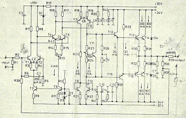
Original 1973 Otala Schematics
Note the hand-drawing on the schematic. First attempts at traditional current
limiting can be seen — this was soon discarded. Note also the extra resistors
near the output: the loudspeaker was to be coupled between the output
terminal and the small 0.1 ohm resistor to ground. This was a later idea
(I don’t remember when it was introduced) which would give some current
feedback in addition to the traditional voltage feedback. The effect would be
to make the loudspeaker “invisible” to the amplifier.
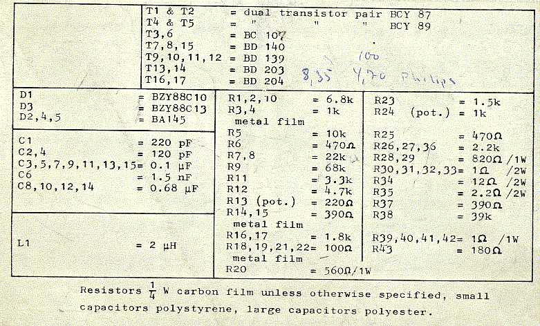
Note that you can see the prices on the transistors here: NOK 4.70 in qty 100
for BD203/204. Cheap transistors!
The Real Electrocompaniet Schematics
The schematics of the real EC 25W amplifiers, shown below, are taken from a
service manual, with full acceptance from Per Abrahamsen of Electrocompaniet.
He approved of, and even supported, the idea of making these schematics
public through this site, in order to cover the history of Electrocompaniet.
Note that the schematic layout is very close to the original, except for the
changes to the compensation networks (look at the emitters on the
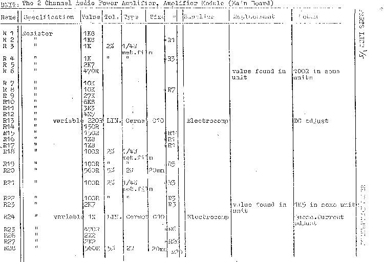
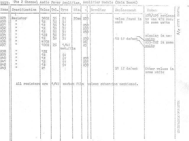
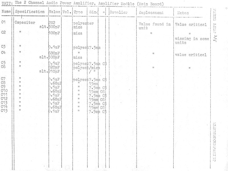
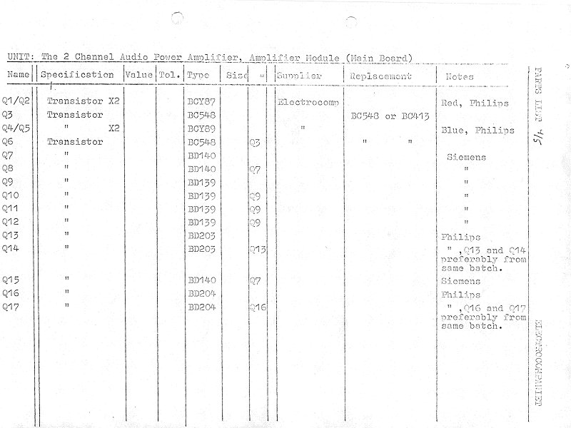
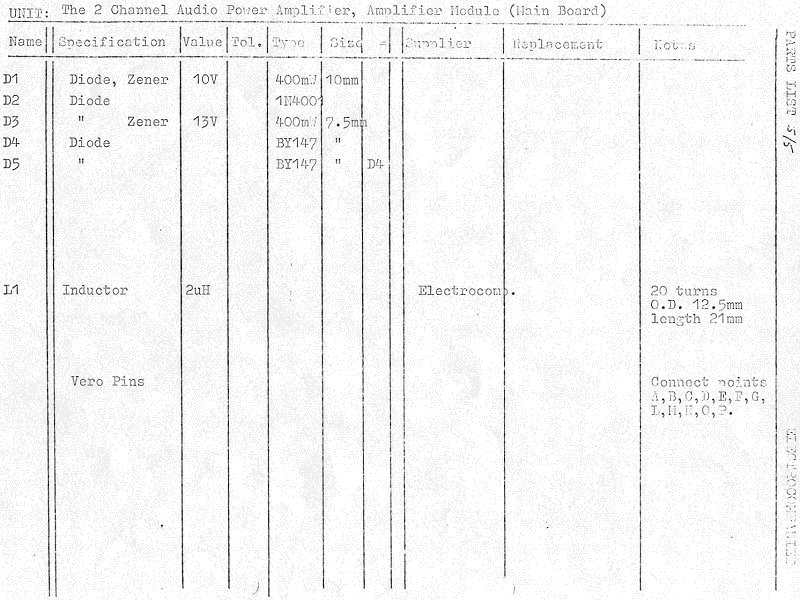
differential voltage-amplification pairs). The major changes can be found by
looking at the component lists below, which apply for amplifiers with serial
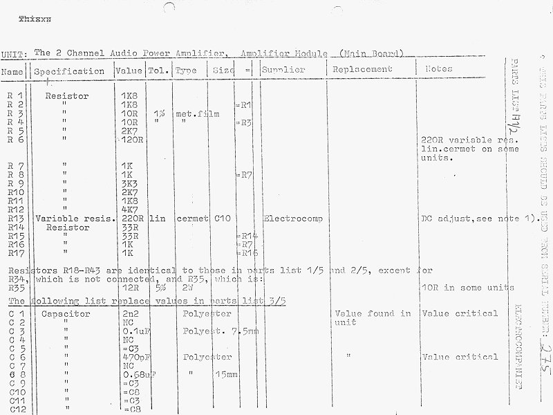
numbers below 275. The component list for serial numbers above 275 is covered
in an addendum further down. You’ll need both lists,
cross-checked, to get the full picture.
(This scan is a bit rough — a better one may come later.)
Above 275
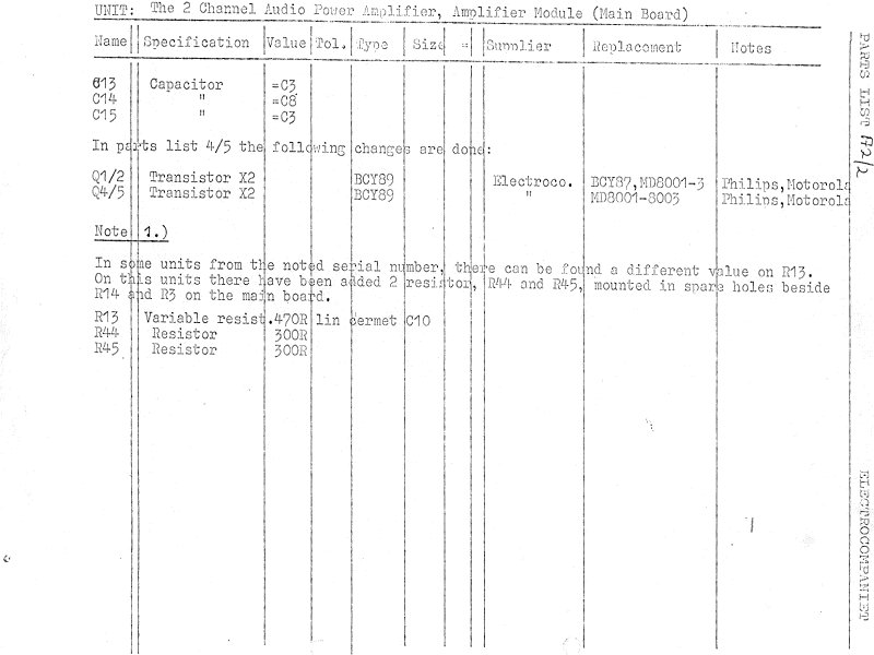
Component lists for serial numbers above 275, the Great Change:
So — this covers it. No further change was done to these amplifiers by
Electrocompaniet. Well, not quite true — I did some further modifications
after I left Electrocompaniet; see the NRF modifications
page.
I’m not quite sure how many amplifiers were made, but by mid-‘77 we had
reached serial no. 275, which took 2 years to reach. From then I believe
approx. 50 units were manufactured each month, until approx. 1981-82, when
Electrocompaniet introduced the Ampliwire series, which replaced the 25W
amplifier. This means there could be some 2000 amplifiers around. Perhaps Per
knows more.
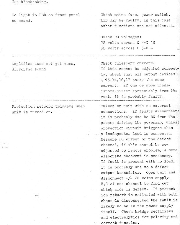
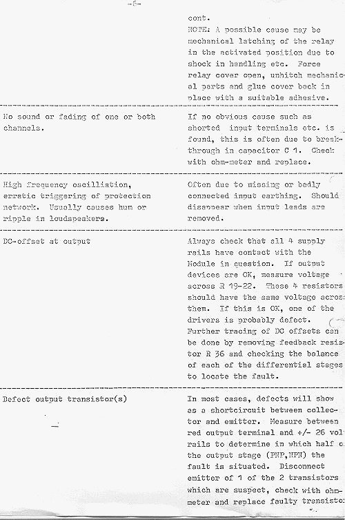
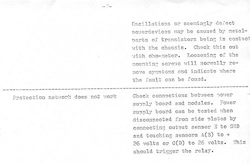
This page is intended to help you if you’re going to service your amplifier.
Electrocompaniet still services their old amplifiers, and I still service
those I modified between 1979 and 1983 — however, the process may be slow (too
much other stuff to do), so if you’re good with a soldering iron and have some
instruments to help you along, this page together with the schematics may be
what you need.
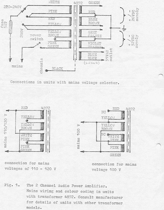
The transformers were also special:
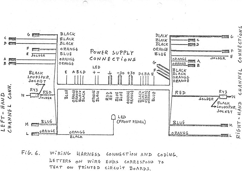
And the wiring harness:
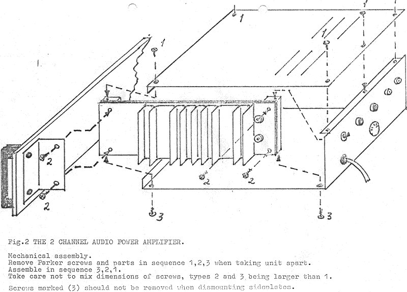
We thought we ought to have those exploded mechanical-assembly-view drawings,
like the Japanese manufacturers did. What do you think about this?
I will put up schematics and other material on the preamplifier as well.
However, first a few tips, based on real cases I’ve had in recent years.
“Scraping” in the volume control
This is due to DC leakage through the coupling capacitors, out from the RIAA
stage and into the line stage. Replace the RIAA output electrolytics with
2.2 µF polyester, and the line-stage input capacitors with 0.68 µF polyester.
Remove the 100k loading resistors.
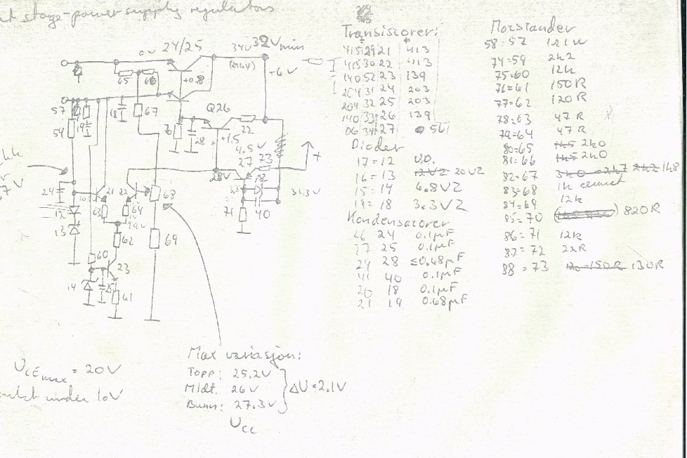
The Regulated 25W Power Amplifier
We noted early on that the power supply had a significant effect on the
sound. We decided to implement regulated power supplies for the amplifier.
I’m not quite sure when we did this, but it might have been sometime in ‘76,
possibly ‘77. We did it straightforward — no switching, no nonsense, only
linear regulators. Hot? Yes, indeed!
I’ve had some trouble locating the schematics for the regulators, but I
believe I’ve found them. It’s possible that the ones shown here are
preliminary schematics — the design never made it into production, so I’m not
quite sure if any other version ever existed.
Only a couple of these amplifiers were ever made, and one of them was
returned to me for service a couple of years ago. Sadly, it was by then
beyond repair.
The amplifier has two sets of supplies, one for the pre-stages and one for
the output stages, so two sets of regulators were needed.
Note the Q27 emitter — it should be coupled to the unregulated pre-stage power
supply. Q27 acts as a current generator and needs some voltage headroom. Note
also that there are no current limiters, so if the regulated output was
shorted to ground, blue smoke was the result!
The transistors are listed with only numbers: 139/140/203/204 are BD, and 413
is BC. All BD transistors were heatsinked — in fact, they were mounted onto
the bottom plate of the amplifier!
Chapter 100
Post-EC / NRF
Post-EC / NRF (Norsk Radiofabrikk)
Not EC factory work — my own modifications and designs from the NRF era
(1979 onward), after leaving Electrocompaniet.
After I left Electrocompaniet in 1979, I tried to start up a new audio company
in Asker together with two good friends, Paal Rasmussen and Espen Evensberget.
We called the company “Norsk Radiofabrikk” (in
English, the Norwegian Radio Manufacturing Company). We wanted it to sound
old-fashioned, and really had a lot of good fun with this. However, our own
original designs never made it into reality. In 1980, or thereabouts, we
started to modify EC amplifiers. We modified between 50 and 100 amplifiers,
and a somewhat lesser number of preamplifiers. The sound improvement was very
good — not too surprising, since I knew these amplifiers in and out. Later we
did some 50 amplifiers from the ground up, called the Special Version — the
modification taken to its logical end. The components for these amplifiers
came partially from Electrocompaniet. I don’t think Per liked it, but I also
don’t think he really minded — if he had, he wouldn’t have sold us components,
like cabinets and so on.
I have had some trouble locating all the schematics and component lists —
don’t really know where I have (mis)placed them. However, I have redrawn the
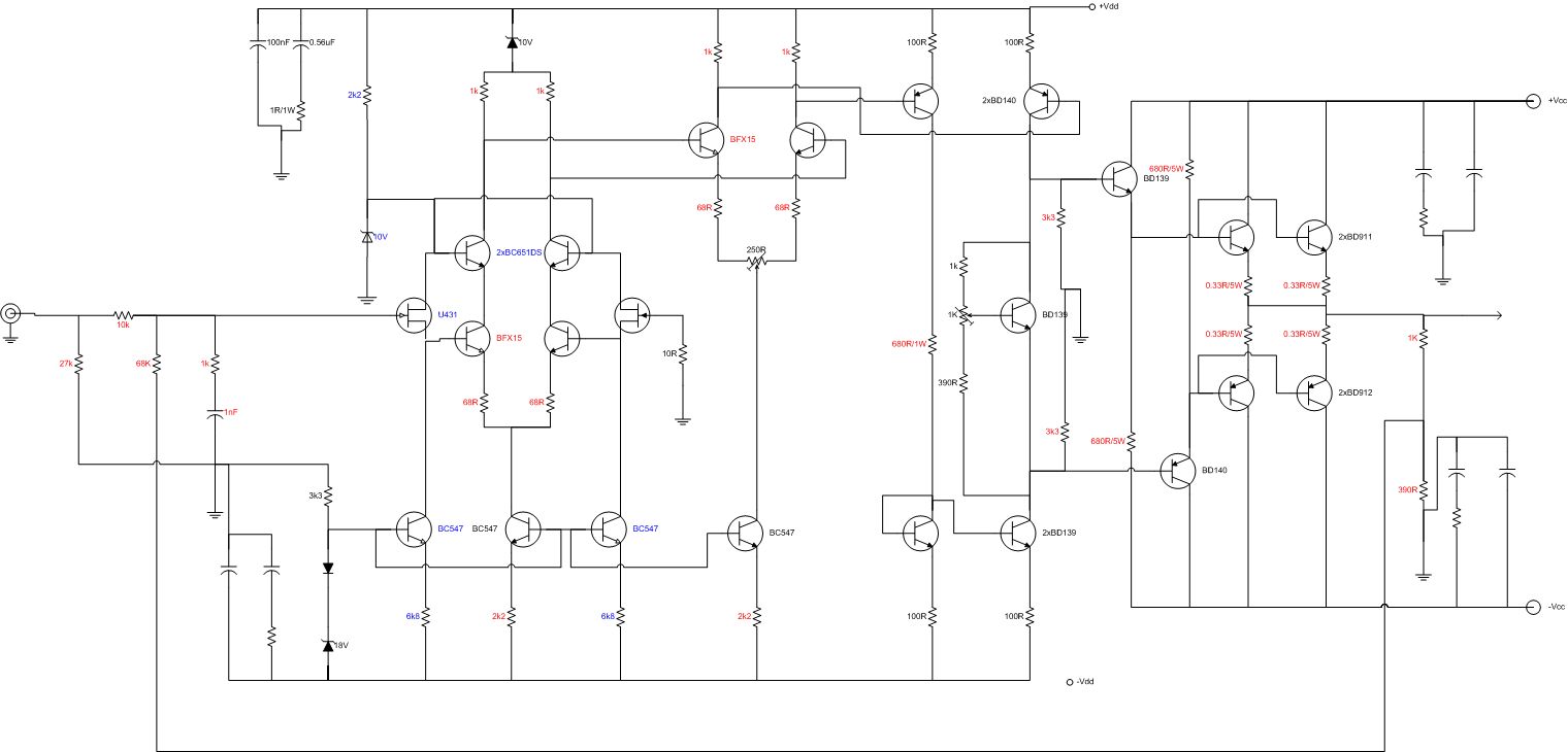
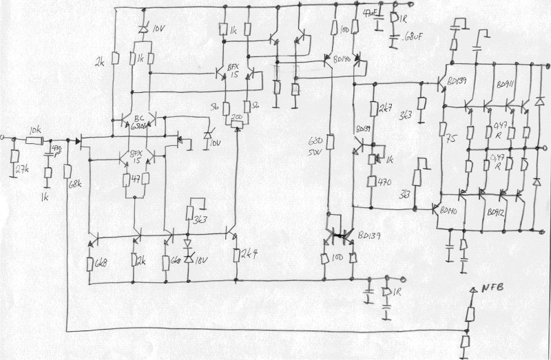
schematic for the modified amplifier below. Please be aware that the
schematic is not to be used for commercial purposes without my permission.
All private use is encouraged.
Components with red values are changed, components with blue values are new,
otherwise equal to original values. Please get in touch regarding proper
frequency compensation of this amplifier.
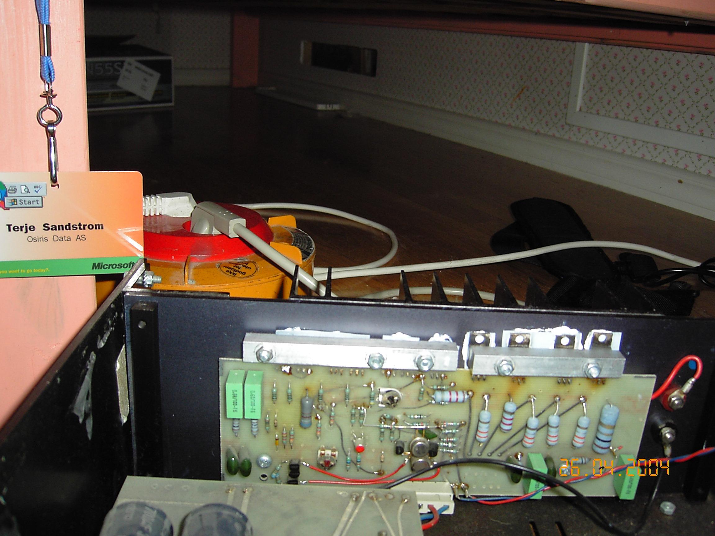
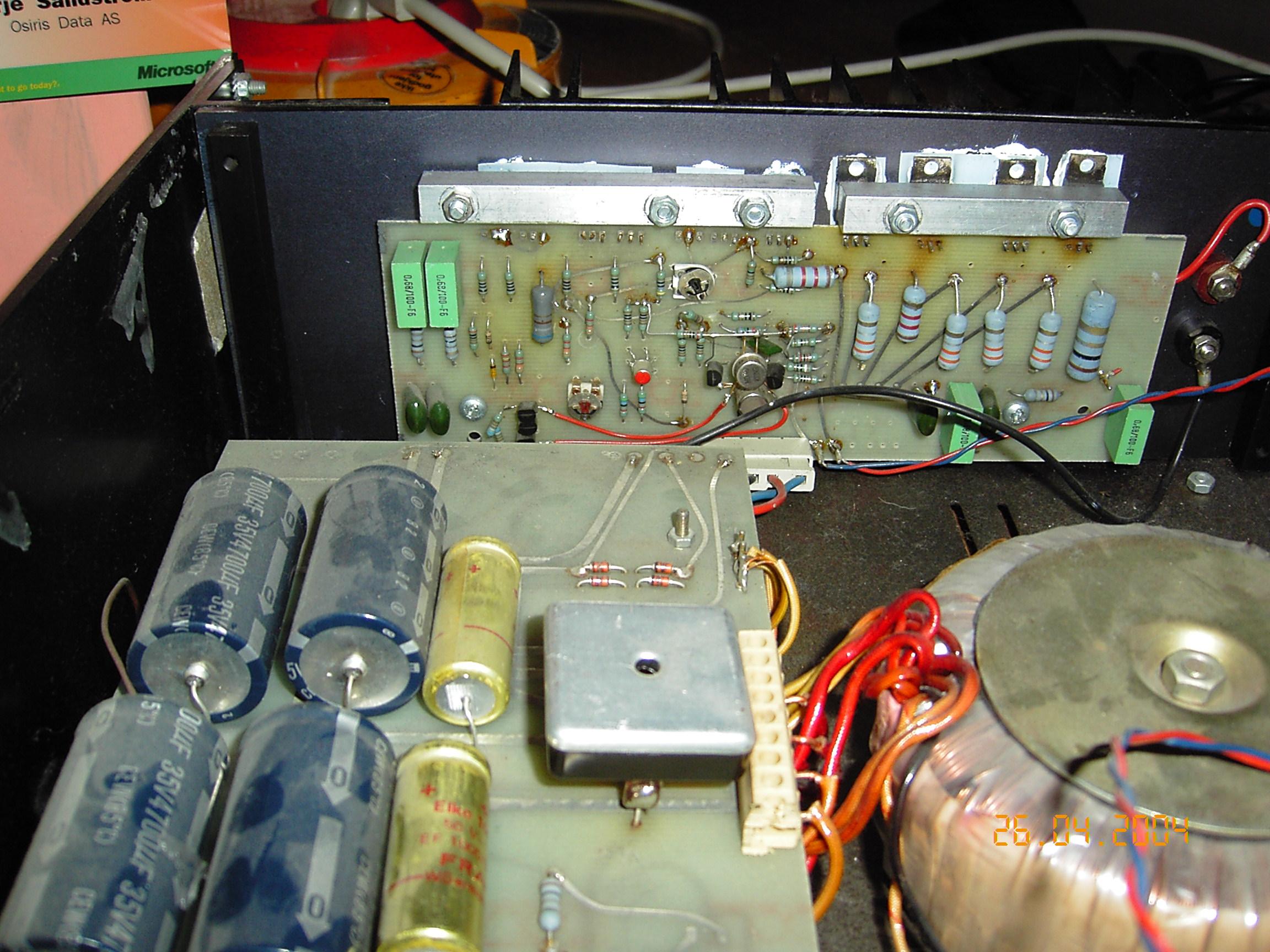
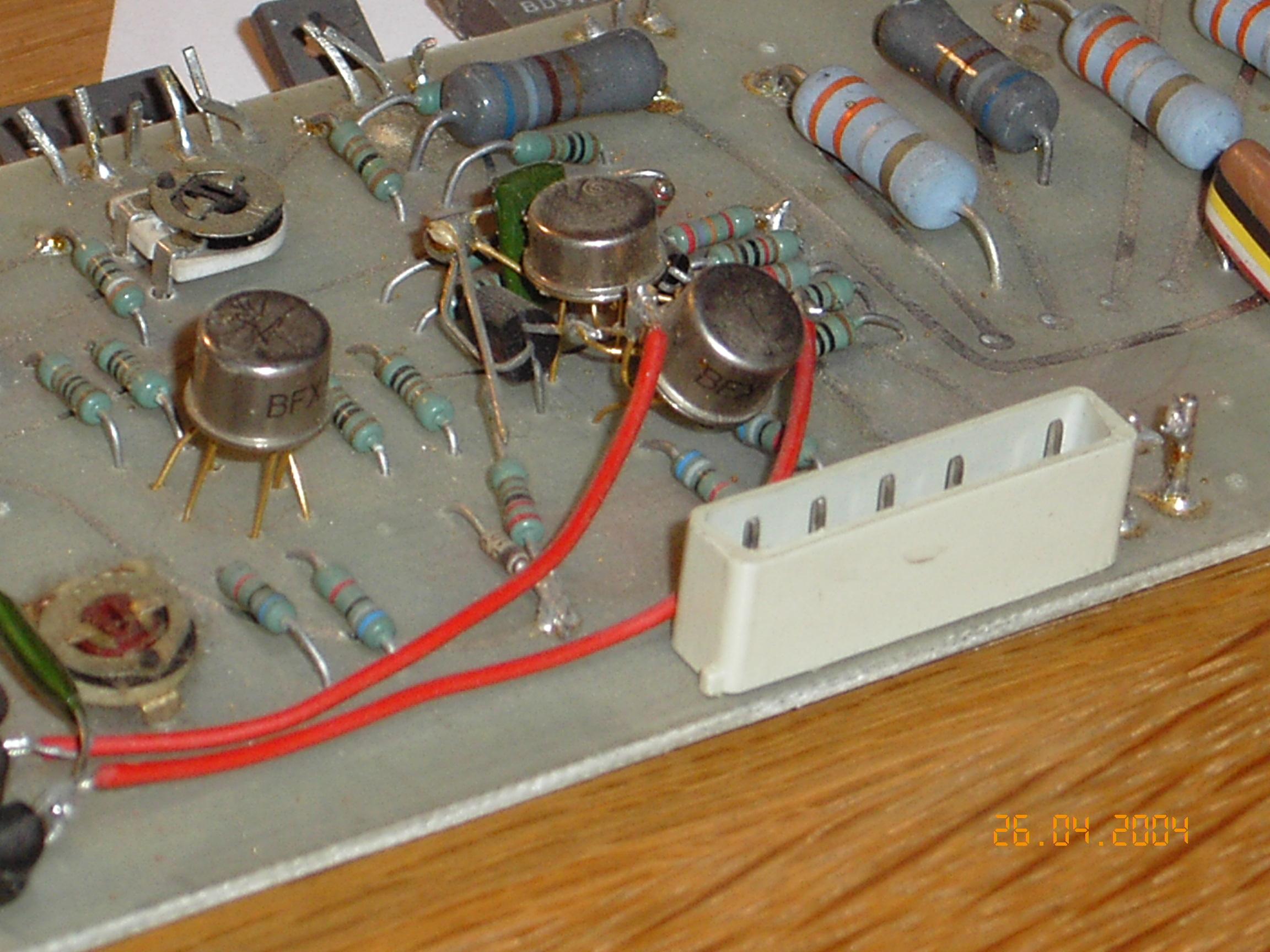
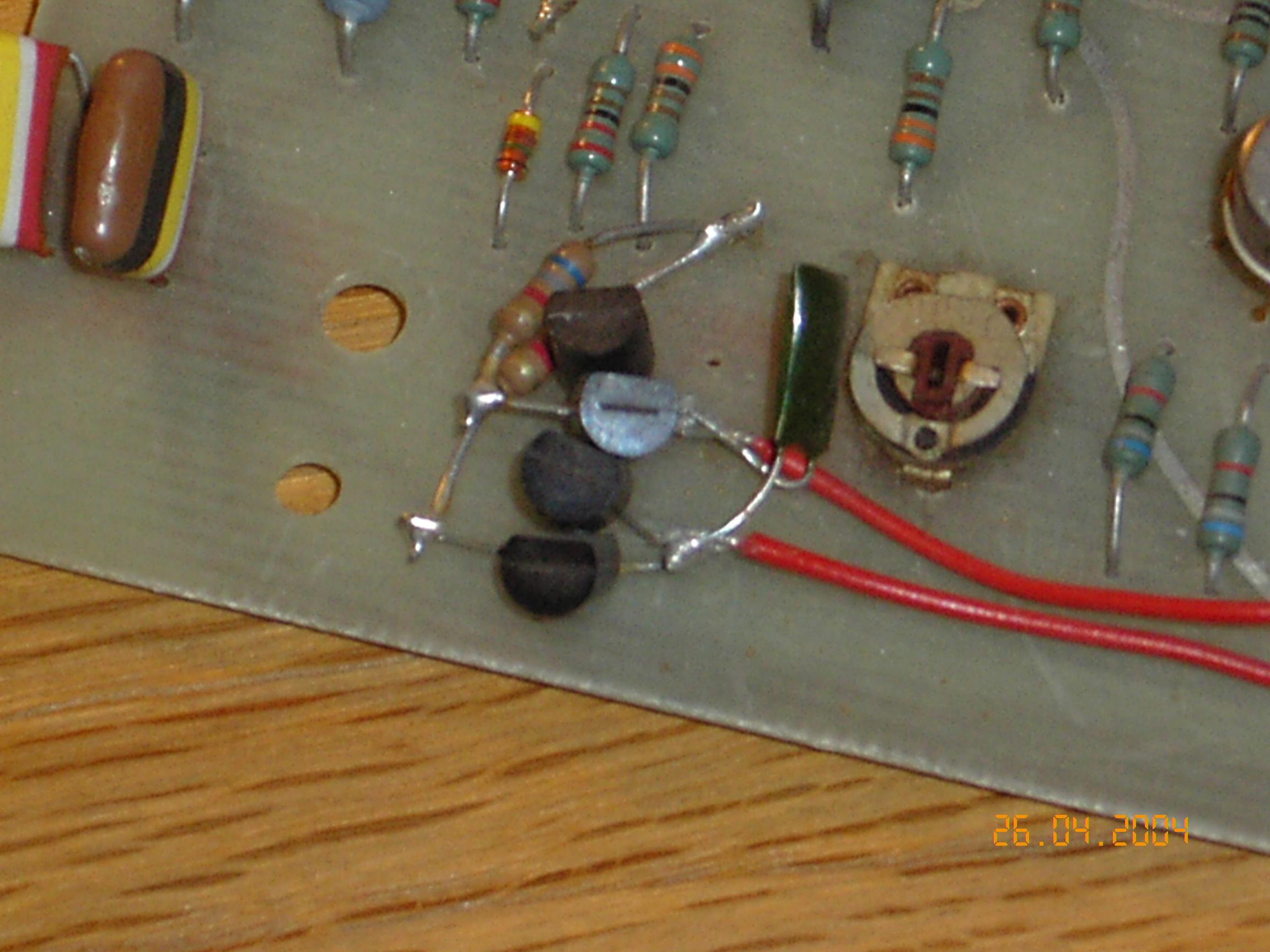
I’ve also included some pictures of the modified circuits below, so that you
can see for yourself how we did the practical part of the modifications. Note
that none of the traces were cut on the circuit board — all new components
were wire-mounted (“bird’s nests”). Not the prettiest thing, but it sure
works.
The modification significantly reduces the distortion of the amplifier,
bringing much more clarity to the midrange, a tighter bass, and a smoother,
less harsh top.
(A later note also mentioned a further schematic variant that popped up —
apparently a later version that also never made it into reality, with
component values and general setup equal to the modified ones described
here, but with an extra double pair of output transistors and emitter
followers added before the third stage. That particular schematic image
itself hasn’t survived.)
The Special Version
Later we did some 50 amplifiers from the ground up, called the Special
Version — the NRF modification taken to its logical end.
Note the heavily reduced values of the output-stage emitter resistors — down
to 0.33 ohm from 1 ohm! This reduces the AB nonlinearity, as described in my
1982 AES paper.
Note also the changed input stage, with a JFET differential pair as a source
follower. It was found that the bipolar input stage added distortion caused by
its nonlinear input base current acting on the input resistors. (Which again
shows: when we reduced the input resistors from 6k8 to 2k2, we heard a sound
improvement and believed it was caused by improved frequency-response behavior
above 20kHz — it may have been the 10dB distortion reduction that we heard!)
To reduce this distortion further, the JFET pair was added. Further, a cascode
pair was added to eliminate the Miller effect and the nonlinear voltage
modulation of the critical first stage.
The gain distribution was also changed — the 3rd stage gain was increased by
raising the load resistors from 2k2 to 3k3. More gain was needed to increase
the overall feedback to 40dB. It was found that increasing this particular
point (3rd stage) was the less critical of the options. However, we got
slightly more relative modulation effect on the 3rd stage than we wished for.
All in all, approximately 100 amplifiers were modified, and an additional 50
Special Versions were made.
By the end of the ’80s and the beginning of the ’90s, I tried a few more
changes to the amplifier design, which never made it beyond the lab bench.
Only one amp exists with these modifications. They included emitter followers
added before the 3rd stage, to reduce the modulation effect mentioned above.
Modification photos
(Captions translated from the original Norwegian file names.)
1982 Preamplifier Schematics
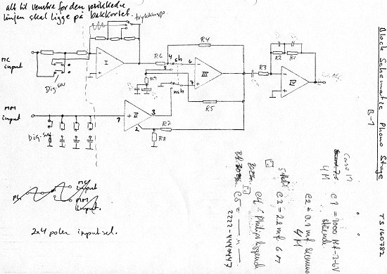
This is the phono stage, handling both MM (Moving Magnet) and MC (Moving Coil)
pickups. The design uses active RIAA compensation, which was untraditional for
the EC design — up to this time it used passive high-pass and active
low-boost. The gain stages are designed to handle the active feedback, and
note (!!!!!), the active RIAA compensation used shunt feedback. A tough
job to calculate, but when that was done, it worked wonders!
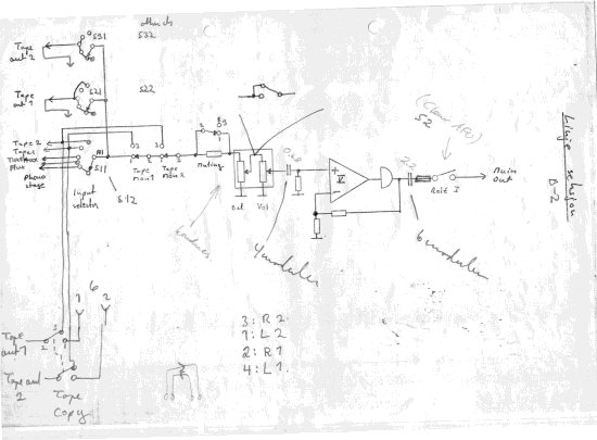
The line-stage section is more traditional, with a normal series-feedback
line stage. Note the extra buffer on the output.
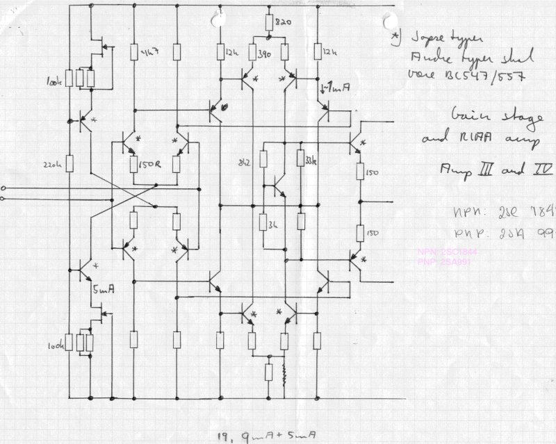
For both block schematics above, note the roman numbers inside the
amplifiers, denoting the particular gain block used.
This drawing shows gain blocks 3 and 4. Note the completely symmetrical
design. The other gain stages also used an ingenious method of utilizing all
the current from the last differential stage. Also note the current
generators — ever seen something like that? Well, it works!
Details on compensation and other design choices will be described further
in a later write-up. Don’t try to build the gain stage as shown above without
that context — smoke will arise. Be patient.
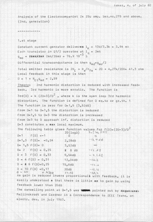
Calculations on the 25W Amp
The following image is the first of an analysis done on the 25W amplifier.
The date, 4 July 1980, indicates that this was done after I left EC (which
was in ‘79, at least on a full-time basis — after a short break in ‘80 or so,
I returned on a consultancy basis to do more work for them until sometime in
1982).
I will upload the whole analysis. For those technically inclined, it should
be interesting — lots of similar analysis was also done earlier. I got the
feeling that many people believed we were only some kind of non-serious
hippies. Well, in a way we were outside the establishment, but we did our
mathematics! Also note the point made at the end of the note, saying that
feedback below 20dB is no good idea when it comes to distortion.
Chapter 30
Theory
The theory of the Otala amplifiers, and thus the basis for the Electrocompaniet
amplifiers, has been detailed in many papers, mostly by Matti Otala, but also
by several others. At Electrocompaniet these theories were extended, and a
theoretical framework for our amplifiers was established. The following pages
give you an insight into both the original theories by Dr. Matti Otala, and
also the theories built up in the first years of Electrocompaniet. Some of the
thoughts are solely mine, however — don’t assume that Electrocompaniet of
today will vouch for all I say here :-)
This is the original outline for the Theory section. Most items below were
only ever sketched as topic headings on the old site and never actually
written up; they’re kept here as a record of the plan, marked (not yet
written).
On TIM, DIM, nonlinearity and distortion
TIM — this was the starting point of Otala’s theories, and his own idea
from the beginning. In the early ’70s many people had already noticed that
the sound of the new transistor amplifiers was inferior to the sound of
tube amplifiers. How could that be, when the transistor amps had less
distortion than the tubes?
DIM — what it is, and how it relates to TIM. This was when everybody
tried to find measurement methods. (not yet written)
The debates and the quarrels — but Otala was right! (not yet written)
“All distortions are equal, but some are more equal than others.” That was
the feeling at Electrocompaniet at that time, and the beginning of an
understanding of how these distortion mechanisms interacted, and how they
affected the sound — and that the basis of all distortion is nonlinearity.
The nonlinearity is the source, the distortions the symptoms. (not yet
written)
A theoretical framework for building good-sounding amplifiers
A theory of single stages — a single stage is the basis
for all amplification, and at Electrocompaniet a model for the single stage,
and “our way”, evolved.
A theory of multiple stages — multiple stages put together do not behave as
N times a single stage; they interact, and in many cases even counteract.
(not yet written)
A theory of feedback — many people are either pro-feedback or fully against
feedback. At Electrocompaniet we learned to live with feedback in all forms,
local and loop, and learned how to get it as a friend and not an enemy.
(not yet written)
Output stages — that current, what does it do? (not yet written)
How do we calculate the nonlinearity
Calculations of input-stage nonlinearity — this is
simple, once you know how; a table summarises everything.
Calculations of the nonlinearity of multiple stages. This is more
complicated, but by following a set of rules, and abiding by the general
model we use, it is not that difficult. (not yet written)
Calculations of distortions — one thing is the nonlinearity, another is how
much distortion of the different types your amp will measure. (not yet
written)
Designing for lowest distortion. Note that there very seldom exists one
optimum point — there are just too many variables, so you have to use some
creativity and a feel for what’s going on. (not yet written)
How the frequency plane and time plane interconnect (not yet written)
Time-response behaviour (not yet written)
Poles and zeroes (not yet written)
Compensation of an amplifier (not yet written)
Other factors
The damping factor — or output impedance, what is it? (not yet written)
Why there are no simple solutions (not yet written)
Power-supply interaction (not yet written)
RFI — what can it do (not yet written)
The importance of the components (not yet written)
Subsections of Theory
A Theory of Single Stages
The general idea
When you design something, you’re moving your ideas and abstract thoughts
into the real world. Using electronic components, they will never act
exactly equal to your ideas. So the best approach is to approximate their
behavior, and make them work as close to your ideas as possible. Further, if
you choose your models skillfully, you will get a behavior from the device
which very closely mimics what you’re after.
Therefore, the sequence is: Model ⇒ Design ⇒ Measurement ⇒ Listening — and you
circle this sequence until you’re happy :-)
The walkthrough below is rather detailed, to show the general outline of the
procedure. The other derivations are less rigorous.
A model for a single stage
We model a single stage as a voltage-controlled current source. In our ideal
world this means we want an active device working as a transconductance
device. A transistor (and also a tube) is very close to this ideal. But one
has to further improve the circuitry around the active device, in order to
make it behave as closely as possible to this ideal.
What this means is that a perfect transistor, and thus a perfect stage, will
have infinite input impedance, no reverse coupling from output to input,
infinite output impedance, and a finite and constant (with respect to both
the signal and the environment) transfer conductance.
Real transistors are not quite as good as this, but we can improve on the
transistor in order to make it behave more like this ideal. Doing this will
normally make the stage perform better in all respects, but keep in mind that
all rules will turn back on you at a certain stage. There is no such thing as
a free lunch.
If such a stage is voltage-driven, we will reduce the nonlinearity from all
“leakages” back to the input, be it input impedance or reverse coupling. The
dominating nonlinearity will then be the transconductance, which is easy to
control.
A transistor in a common-emitter coupling is the starting point. It has, in
principle, the behavior described above. The following rules exist:
Linear behavior:
Transfer conductance, given by:
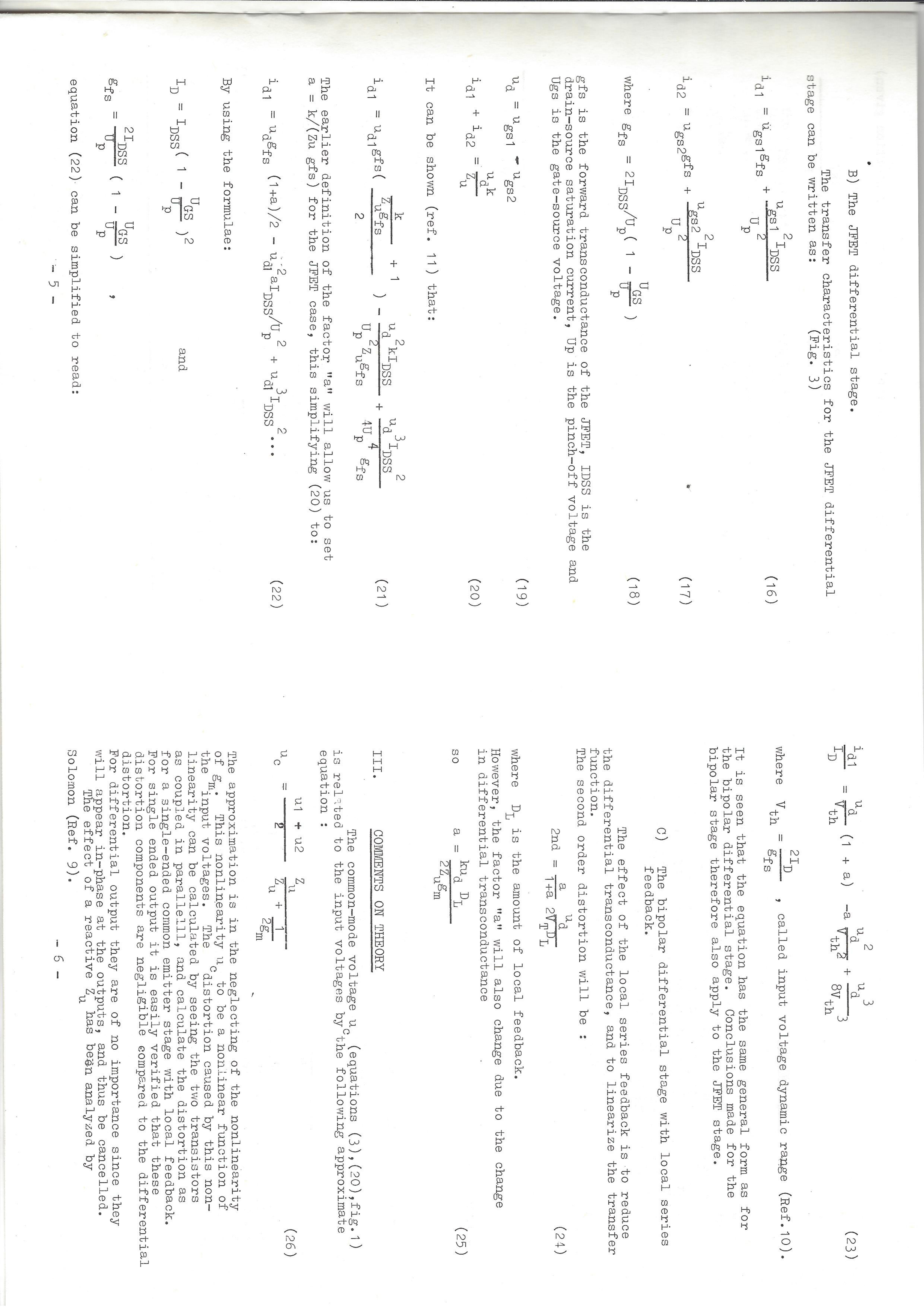
$$g_m = \frac{I_e}{V_T}$$
$I_e$ is the emitter DC current and $V_T$ is the voltage equivalent of
temperature, normally equal to 25 mV — the exact formula is $kT/q$, where $k$
is Boltzmann’s constant, $q$ is the charge of an electron, and $T$ is the
absolute temperature in Kelvin.
The inverse of the transconductance is called the dynamic resistance, called
$r_e$.
Current amplification: $H_{FE} = I_c/I_b$, derived for a particular current
$h_{fe} = i_c/i_b$, which applies for small-signal currents around a
quiescent point $I_c$.
Input impedance: $r_{in} = h_{fe} \cdot r_e$
The dominating nonlinear mechanism lies in the transconductance. Since this
is a single stage (not a differential stage) it will generate a smooth series
of harmonics (if stimulated with a pure sinusoid).
If the input signal is given as $x$ (where $x$ can be e.g. $\sin(\omega t)$),
then the output $y$ will be:
$$y = a_1 x + a_2 x^2 + a_3 x^3 + \cdots$$
And $x$ is a relative parameter which must always obey $|x| < 1$ in order for
the series to converge. If $|x| < 1$ then it follows that $|y| < 1$. The
output current is $i_e$ and the output parameter is then $i_e/I_e$. The input
signal generating a current of $i_e$ is $u_{in}$, from the formula
$i_e = u_{in} \cdot g_m$. It then follows from the transconductance formula
that the input parameter we seek is $u_{in}/V_T$.
So, given the input $x$, defined as $u_{in}/V_T$, and the output $y$, defined
as $i_e/I_e$ — what do these things mean?
If $u_{in}/V_T$ exceeds 1, then the varying part of the current exceeds the
quiescent current $I_e$, and the stage is clipping. When the stage is
clipping, our formula breaks down. If we want to find the distortion when the
stage is clipping, we’ll have to resort to Fourier analysis.
To make this into a practical case: assume a transistor running at a current
of 1mA. The $g_m$ is then 1/25 siemens (the inverse of ohm, the unit for
transconductance, although “mhos” — ohm reversed — is also used). An input
signal of 1 mV will then generate an output current of 1/25 mA = 40 µA. But
now note: this is the first-order approximation. As can be seen from the
series expansion above, we also have second- and third-order components. The
first-order coefficient should be pretty close to $g_m$, but what are the
other two coefficients?
The real equation relating input voltage to output current is
$I_e = I_s \cdot \exp\left(\frac{U_{be}}{V_T} - 1\right)$, called the
Ebers-Moll equation. $I_s$ is the “leakage” current, but don’t bother about
it — we’ll soon enough get rid of it. We are interested in finding the
equation for the behavior around the quiescent point. We do this by adding
small deviations $i_e$ and $u_{be}$ to the equation above. Resolving this, we
get the much simpler equation: $i_e/I_e = \exp(u_{be}/V_T) - 1$, and its
inverse: $u_{be}/V_T = \ln(1 + i_e/I_e)$. These equations are called the
signal equations, and will be used to get the coefficients for the series
expansion above. We’ll first make a series expansion of the first equation,
and we get:
We now introduce the efficiency parameter $n_i$. The point of introducing
this parameter is to generate simpler formulas for calculating the
distortion, and to gain a better understanding of how the distortion and
other transistor parameters are coupled.
The parameter is defined as:
$$n_i = \frac{i_e}{I_e}$$
For a bipolar stage without local feedback, as the stage discussed above,
$n_i$ is equivalent to $u_{be}/V_T$, where we only consider the linear part
of the series expansion. The equation above can then be written as:
If the input signal is a sinusoid, then the following equations hold (ask via
the about page if you’d like the proof), where $\text{2ndh}$ is
the second-order harmonic distortion, and $\text{3rdh}$ is the third-order
harmonic distortion:
It is interesting to do the same exercise for FET transistors. The result is
a simpler series, with only first- and second-order components. By inserting
the efficiency parameter, one gets the following equation for the FET’s
second-harmonic distortion:
$$\text{2ndh} = \frac{n_i}{8}$$
Half the amount of the bipolar transistor. Some people have argued that the
FET is a much more linear device than the bipolar. This equation shows that
to be only a partial truth — there is only a 6dB improvement.
Local feedback
It is well known that local series current feedback (read: inserting an
emitter resistor) reduces the distortion. The feedback factor can be written
as:
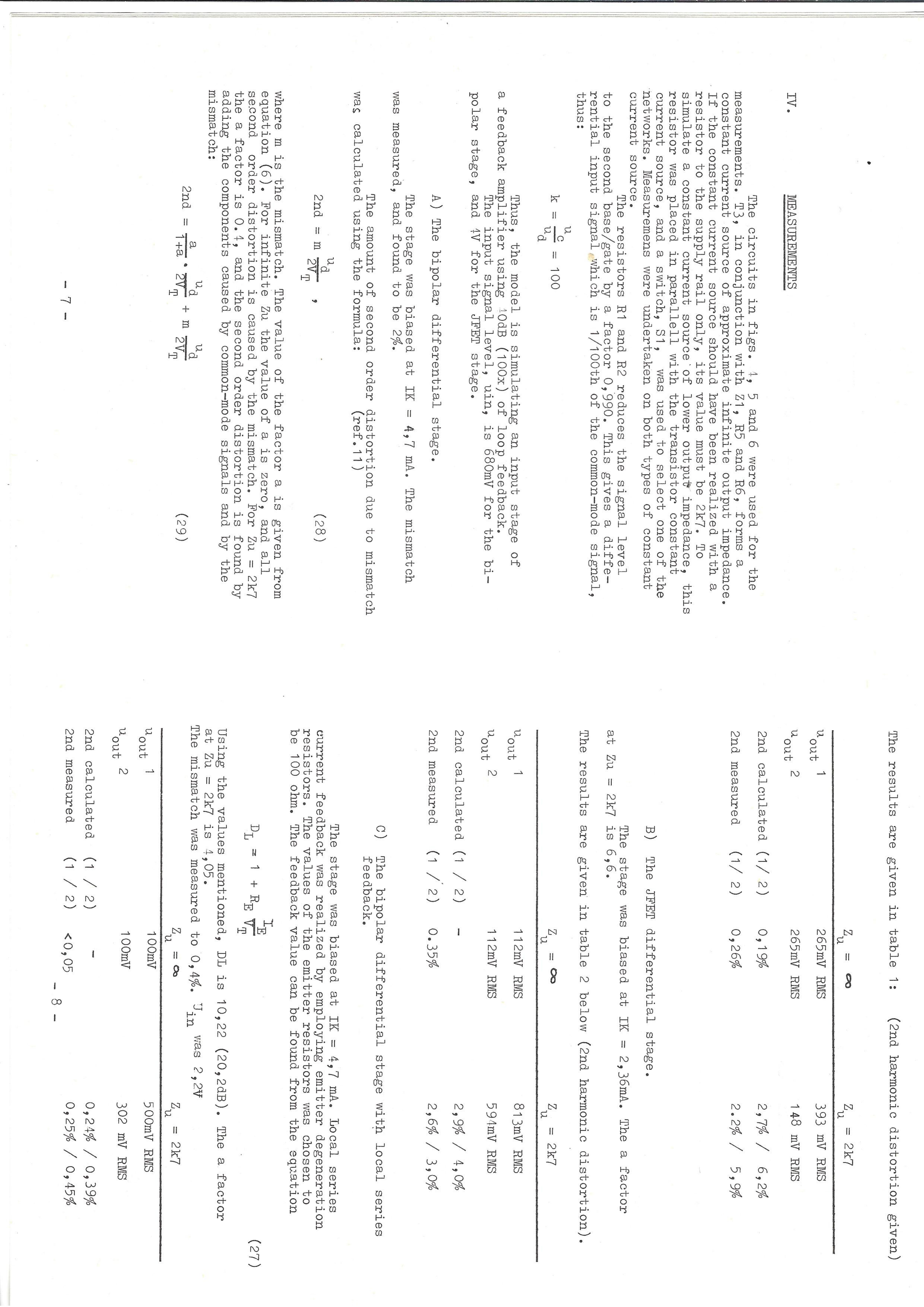
$$D = 1 + g_m R_e = 1 + \frac{I_e R_e}{V_T}$$
and the resulting efficiency/distortion equations are then:
If the current source feeding the emitters has infinite output impedance, $c$
approaches 0. The formula for $c$ is $c = i_k/(2i_e)$. More information on
this is in my AES paper (not yet ported to this site). There used to be an
ActiveX Single Stage Calculator here as well — it’s retired along with the
rest of the site’s old ActiveX controls.
Summary
Stage type
2nd harmonic
3rd harmonic
Bipolar single stage
$n_i/(4D)$
$n_i^2/(12D)$
FET single stage
$n_i/(8D)$
Ideally zero
Bipolar differential stage
$(m+c) \, n_i/(4D)$
$n_i^2/(12D)$
Original derivation notes (kuriositet)
The treatment above uses a simplified “efficiency parameter” shortcut. My
original 1978 handwritten working notes derive the same distortion results
the long way — a full circuit-level analysis in terms of the actual resistor
values ($R_C$, $R_F$, $R_E$, $R_B$, $R_S$), for both a simple stage and the
differential pair, including two appendices (a Taylor series expansion of
$\ln(1+x)$, and inversion of a cubic series). That derivation is not
transcribed onto this page — only scanned here as the original artifact:
The open-loop frequency response is the frequency response of the amplifier
with no feedback — before feedback, or with the feedback network deliberately
broken.
The closed-loop frequency response is the frequency response of the amplifier
with feedback.
These two are closely related. The theoretical closed-loop frequency response
is equal to the open-loop frequency response times the amount of feedback. If
you have 40dB (100 times) of feedback, and an open-loop response of 1kHz, the
closed-loop frequency response is 100kHz.
The formula relating these two is:
$$f_{cl} = \frac{f_{ol}}{1 + A_{ol} D}$$
where $D$ is the feedback factor and $A_{ol}$ is the open-loop gain. The
total denominator expression is what we call feedback.
The open-loop frequency response is determined by the internal compensation
(intended or not) of the amplifier. Many amplifiers are designed with one
stage having a very high output impedance, so the stray capacitance of that
stage’s output determines the open-loop frequency response. For integrated
circuits the open-loop frequency response is either specified, or you can see
it graphically as a function of gain — in the latter case, look at the
maximum gain, which means zero feedback.
Just to remind you: the closed-loop gain $A_{cl}$ is related to the open-loop
gain $A_{ol}$ in exactly the same way as the frequency response, although
inversely.
$$A_{cl} = \frac{A_{ol}}{1 + A_{ol} D}$$
At Electrocompaniet the thinking favored a large open-loop bandwidth. This is
also my opinion, but I feel it shouldn’t be larger than necessary. There is
always a tradeoff, and if you go for too high an open-loop bandwidth, you
reduce the possible amount of feedback you can have. My thinking is that as
long as the open-loop bandwidth is high enough, you should use the rest of
your gain for feedback. This will give you a more optimal design, because the
overall distortion will be reduced.
What determines the open-loop bandwidth
Mostly it is determined by the last voltage-amplification stage. The
collectors of this stage (assuming transistor amplifiers, which these
articles are all about :-)) are connected to the bases of the drivers of the
output stage. The input impedance of these drivers is normally very
nonlinear, and strongly frequency-dependent. This means you can very well get
a major pole here which varies strongly with signal level and the load
(loudspeaker and cables) of the output stage. The solution to this is to
voltage-drive the output stage, thus loading down the amplification stage.
This will also have the effect of pushing up the cutoff frequency at this
point. The EC amplifiers have this pole around 500kHz. The benefits of a
voltage-driven output stage are described elsewhere on this site, including
in an AES paper (not yet ported to this site).
Chapter 40
M.Sc Thesis — Weak Nonlinearities
University of Oslo, 1985
The thesis itself will be uploaded once it’s converted, preferably to
English, and at least from printed form — it was written on a long-forgotten
computer and I’m no longer able to read the diskettes. (Update since the old
site: a scanned copy of the printed thesis exists and will be added here.)
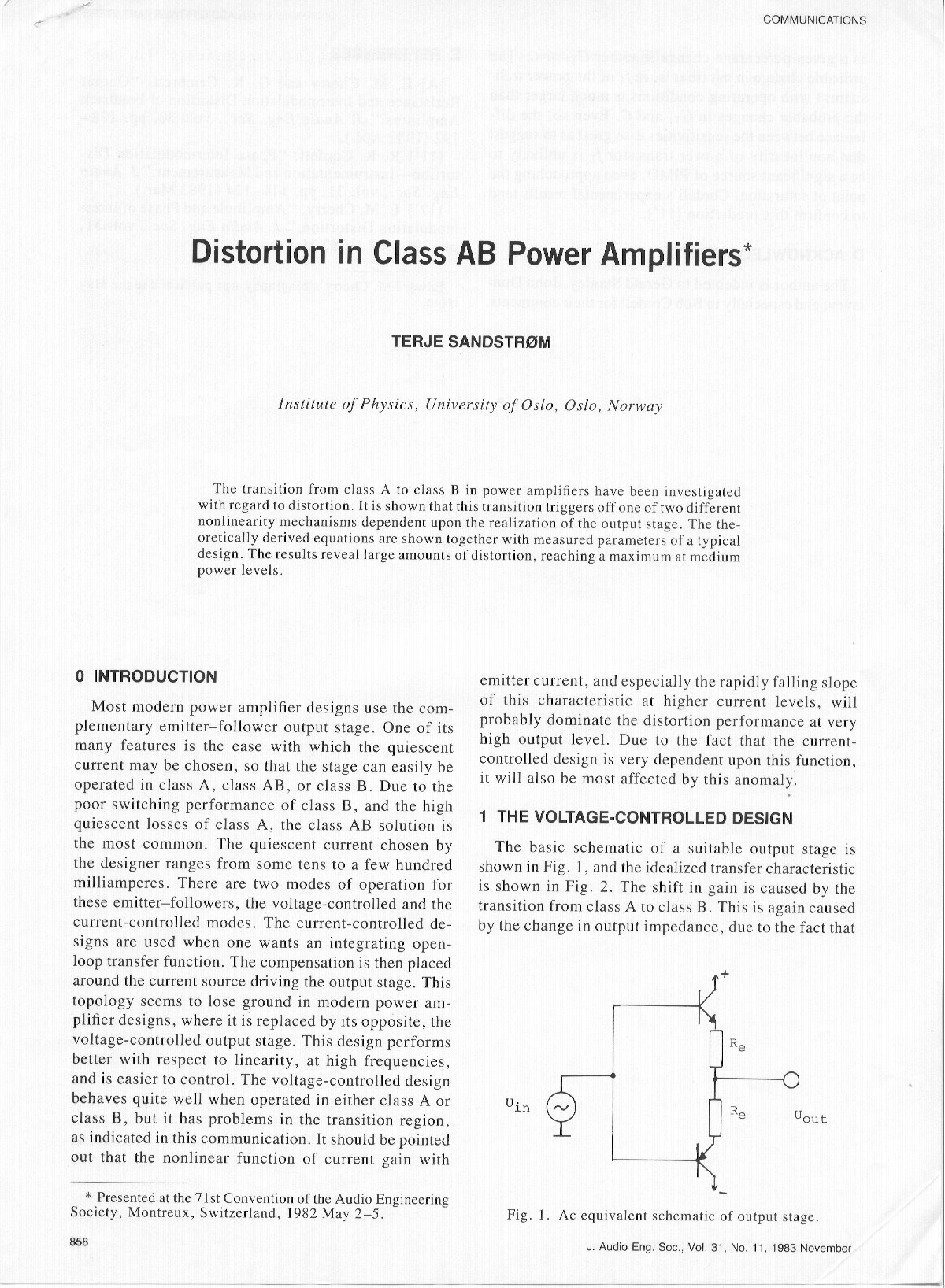
Preceding my master thesis, I presented two papers at AES conventions in the
early ’80s. One of these made it to the Journal of the AES — I’ve scanned it,
so take a look: it’s about class AB distortion in power amplifiers. This
article was also used by the Danish High
Fidelity magazine, which published a follow-up article on it and presented an
amplifier modification of their own, based on this article. I’ve not been
able to locate that follow-up — I believe it was in 1983, possibly the
October issue. If anyone has a copy, I’d appreciate it :-)
Links
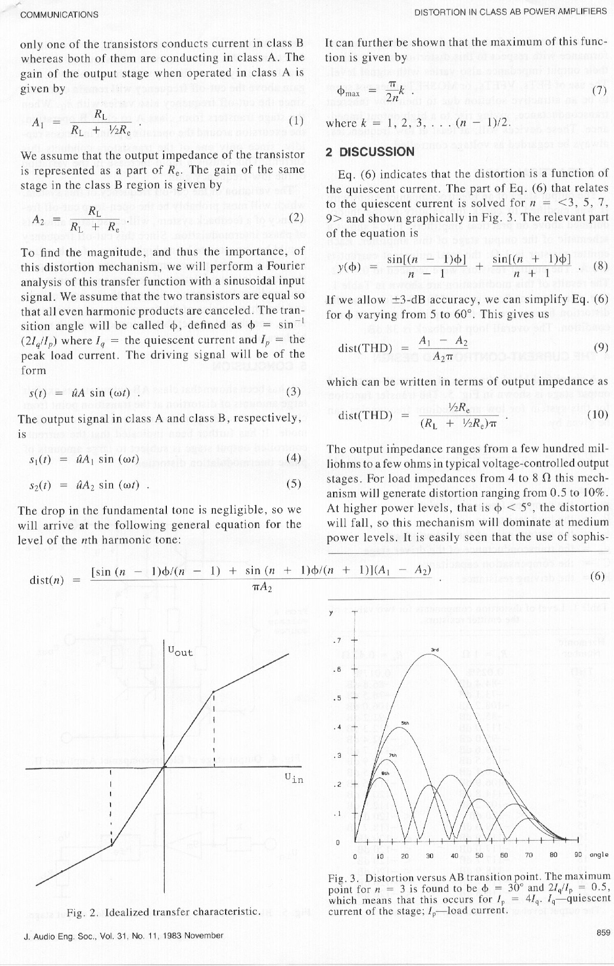
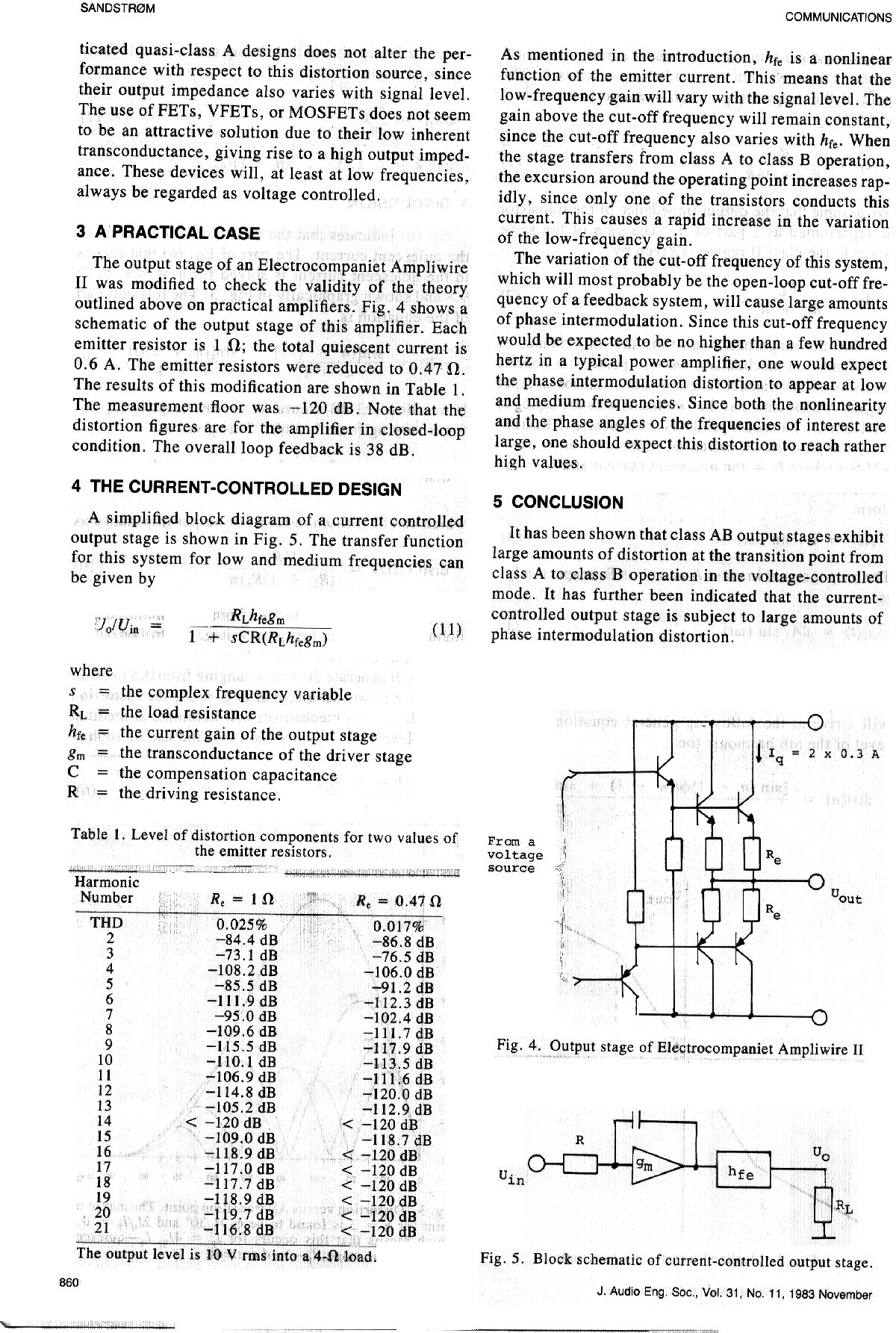
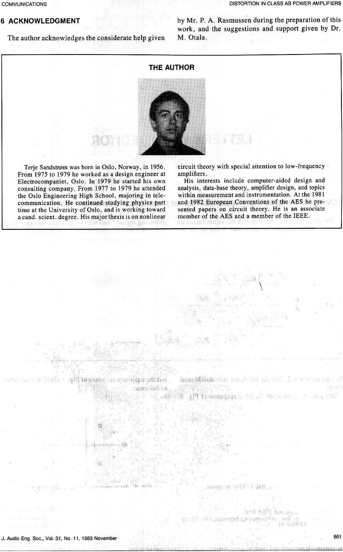
Class AB Distortion in Power Amplifiers —
“Distortion in Class AB Power Amplifiers”, Terje Sandstrøm, presented as AES
Convention 71, Paper No. 1870 (6 March 1982;
AES E-Library), later
published in the Journal of the Audio Engineering Society, Vol. 31, Issue
11, pp. 858–861 (November 1983;
AES Journal Forum).
The second AES paper from this period is still unidentified — if the title
turns up, it’ll be added here too.
Chapter 50
Audio Design
Miscellaneous audio-design work not tied directly to the Electrocompaniet
history: the school amplifier project, cooling-fin calculations, the AES
paper on AB distortion, later prototypes, and other designs.
Two things worth flagging from the source material:
Legacy/abdist.md looked like the AES paper page, but its actual content
was just a generic “site under reconstruction” placeholder — the real
scans lived at Legacy/wiki/ABDist.md instead, which is what got ported.
The cooling-fins overview photo (CoolingFin1.jpg) is referenced by the
old page but was never found in the archive — only the close-up shot
survived.
Subsections of Audio Design
The School Amplifier
Øistein Klevhus, now at FHI (the Norwegian Institute of Public Health), and
myself did a project together at the end of our engineering school. I am
greatly in debt to Øistein, because he was the one who made it possible for
me to go through with that school — I was far too busy with EC, and had far
too little time for school. Øistein came over to me at EC with schoolwork
tasks and other stuff I had to do, and in that way it was possible for me to
get through the school without nearly being present. I am forever grateful
for that!
The amplifier: it was a very special design, fully complementary, and used
matched single field-effect transistors at the input, along with some very
interesting output transistors that had a very low turnover point.
More info on the matching of the input transistors will follow, but for now:
they required manual matching, and it wasn’t easy to find a pair that worked.
Note also the very low emitter resistors on the output stage — this matches a
later paper I did for the AES; see the AB distortion paper.
The matched input JFETs were Siliconix U430/U431 dual n-channel devices —
see the datasheet below.
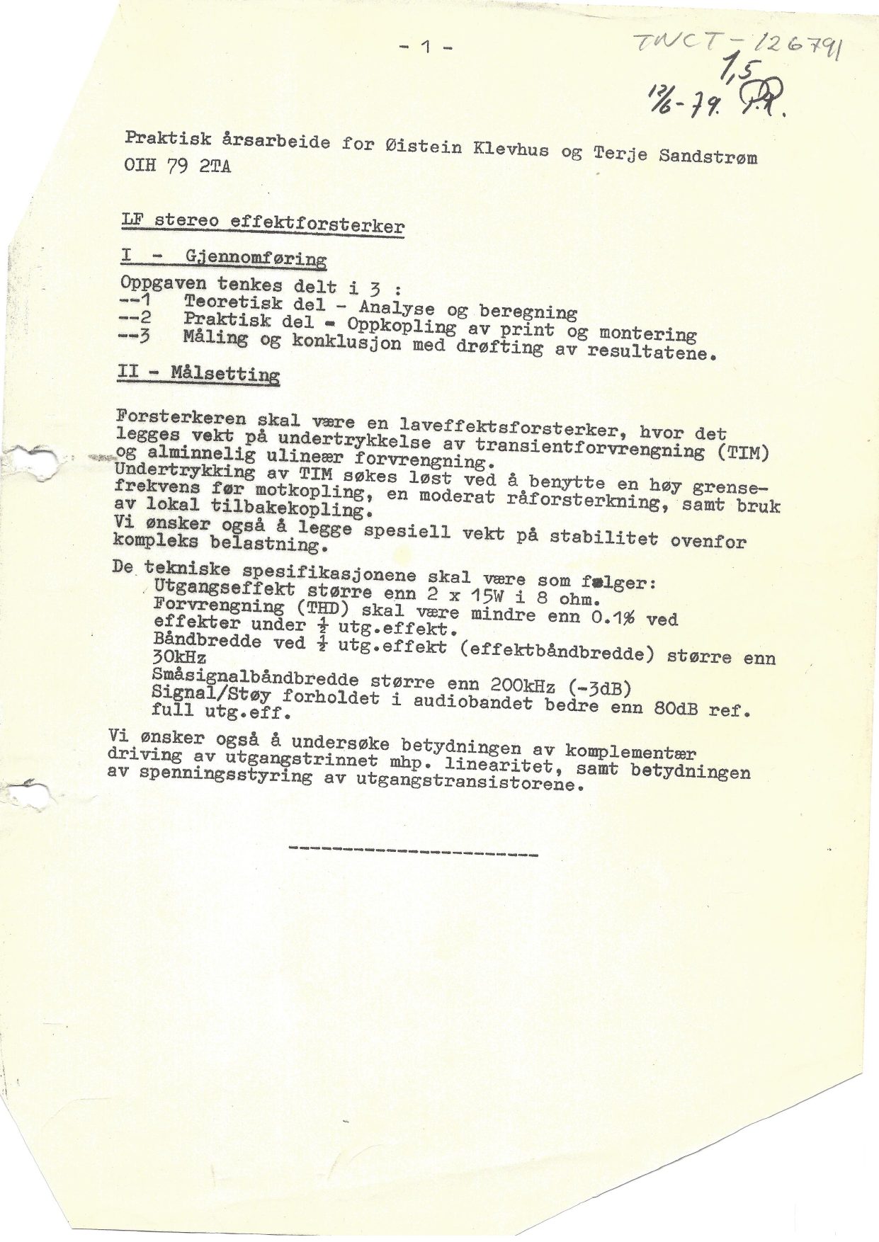
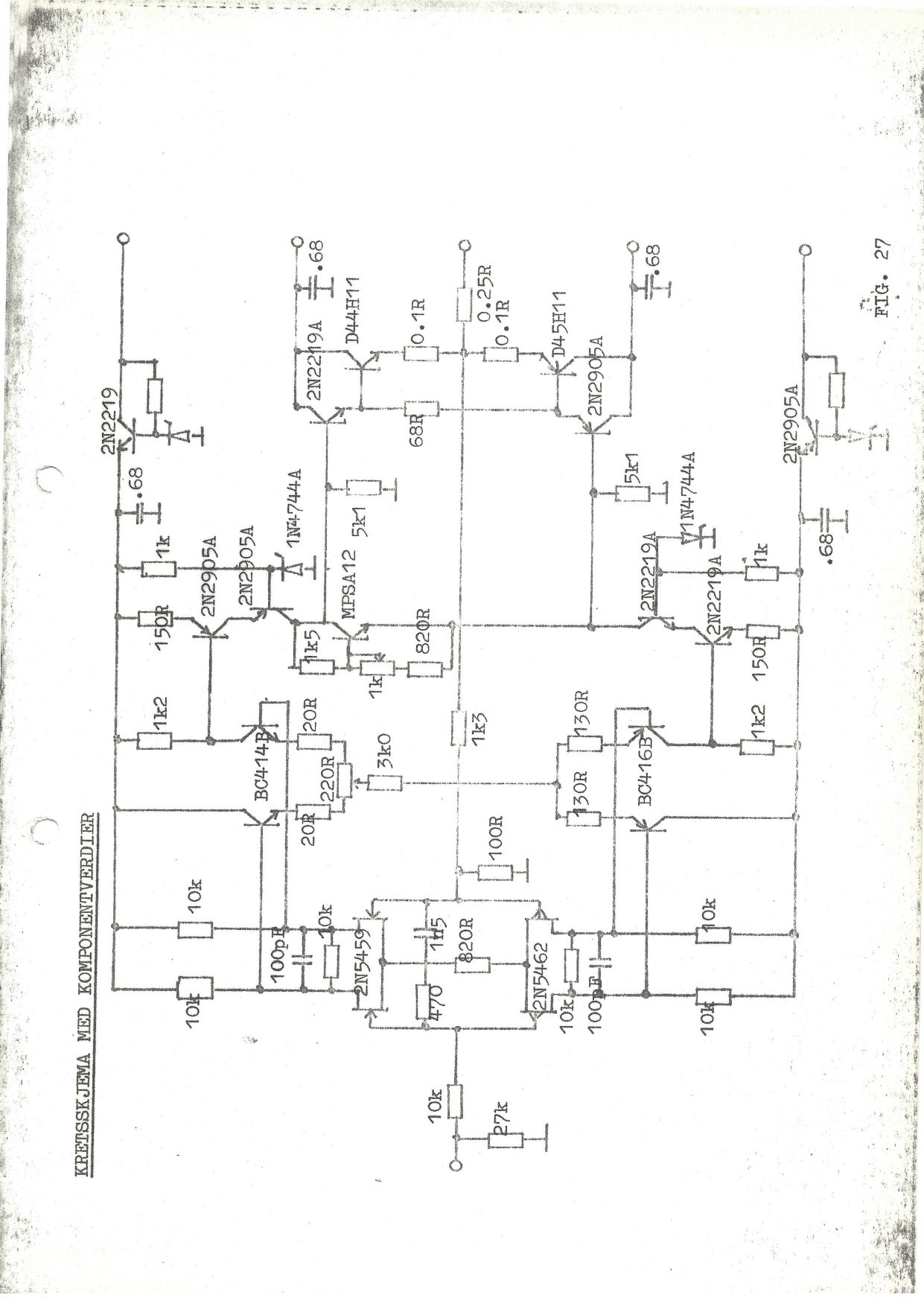
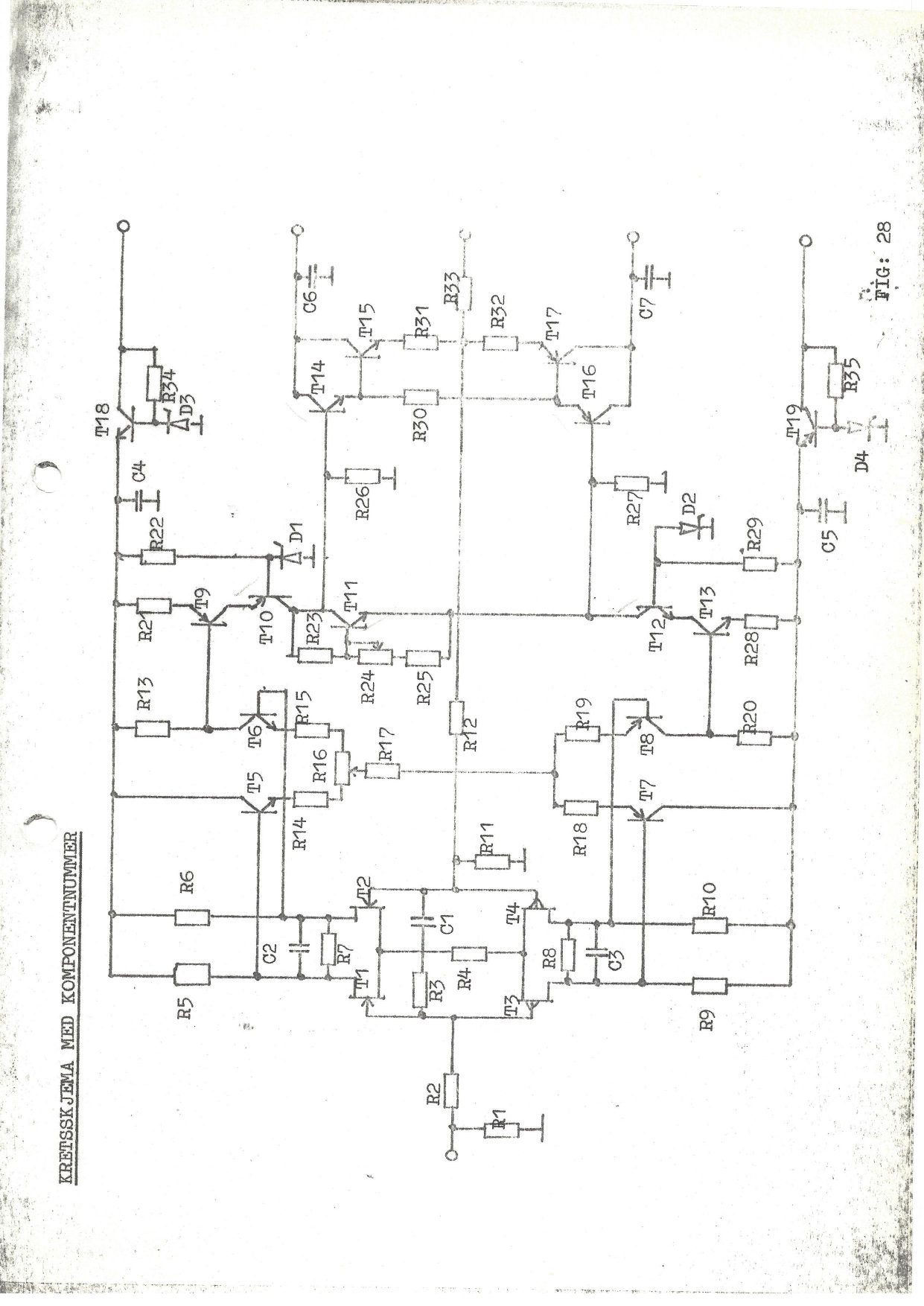
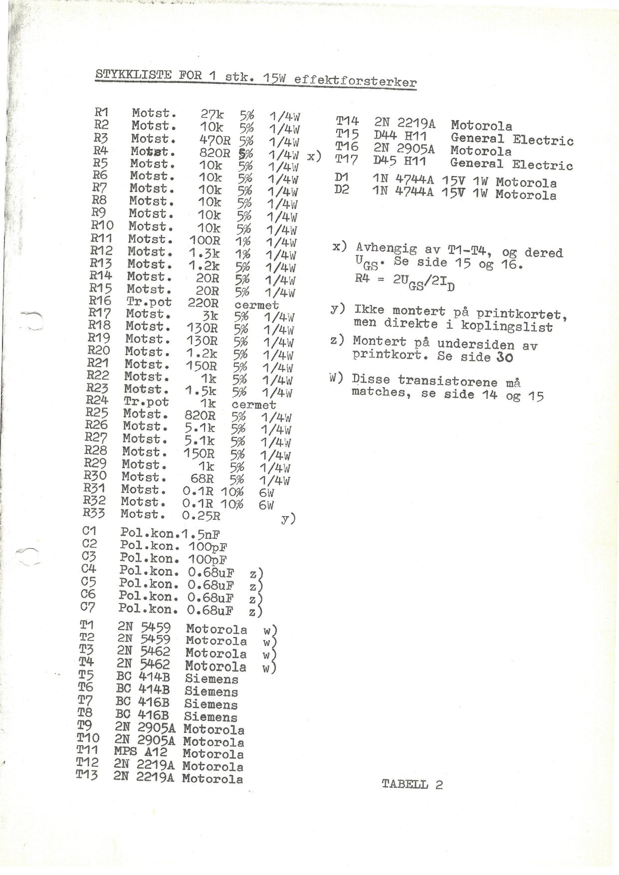
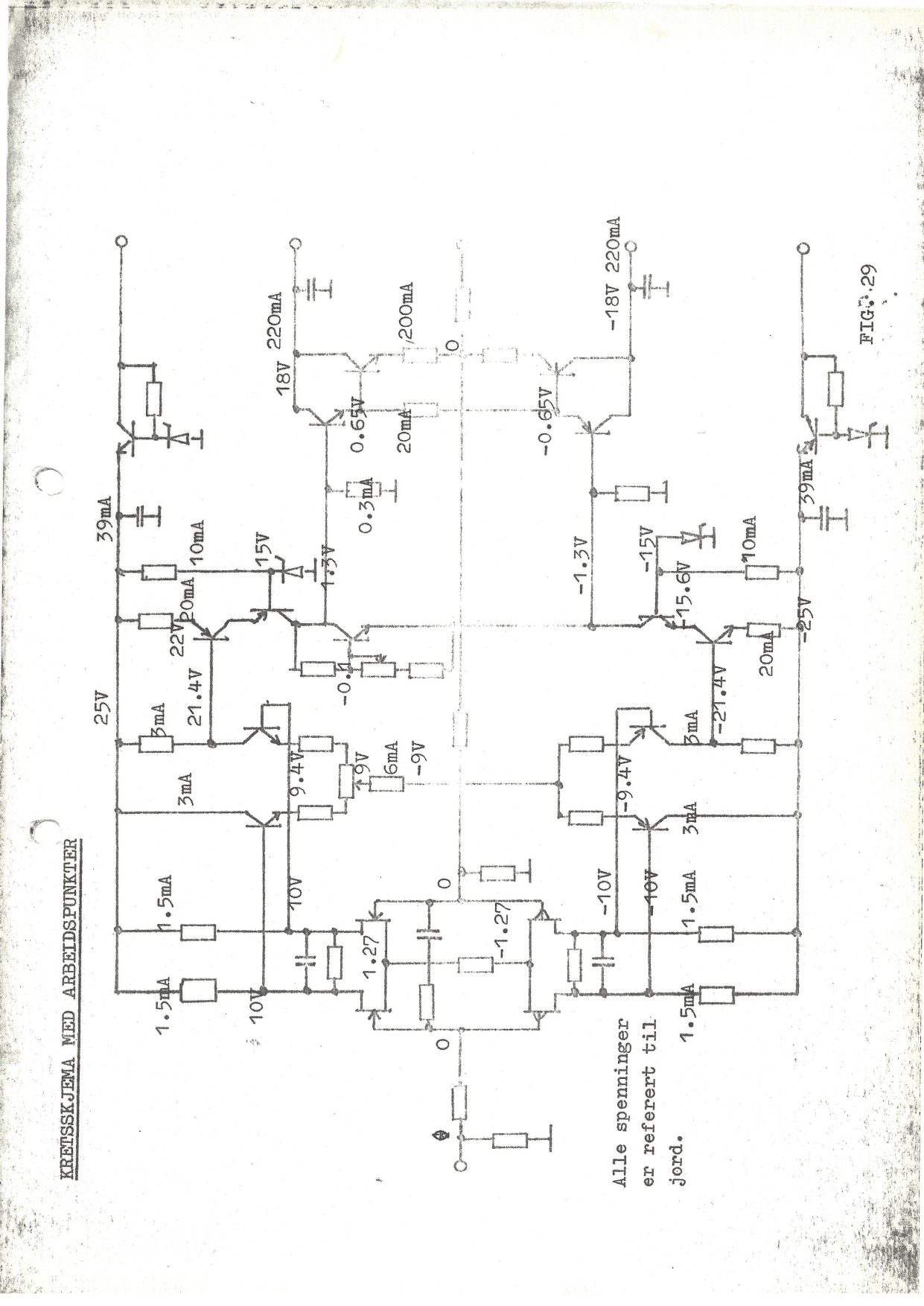
Praktisk årsarbeide for Øistein Klevhus og Terje Sandstrøm, OIH 79 2TA.
LF stereo effektforsterker.
Full transkripsjon av den originale håndskrevne/maskinskrevne rapporten fra
1979. Figurer og tabeller er gjengitt som skannede bilder; formlene under er
satt med MathJax for lesbarhet, men følger originalens notasjon.
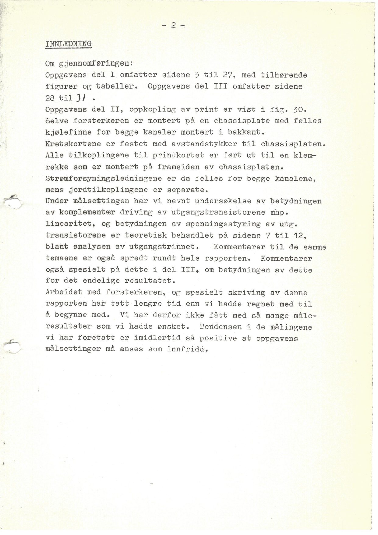
Innledning
Om gjennomføringen
Oppgavens del I omfatter sidene 3 til 27, med tilhørende figurer og tabeller.
Oppgavens del III omfatter sidene 28 til 31.
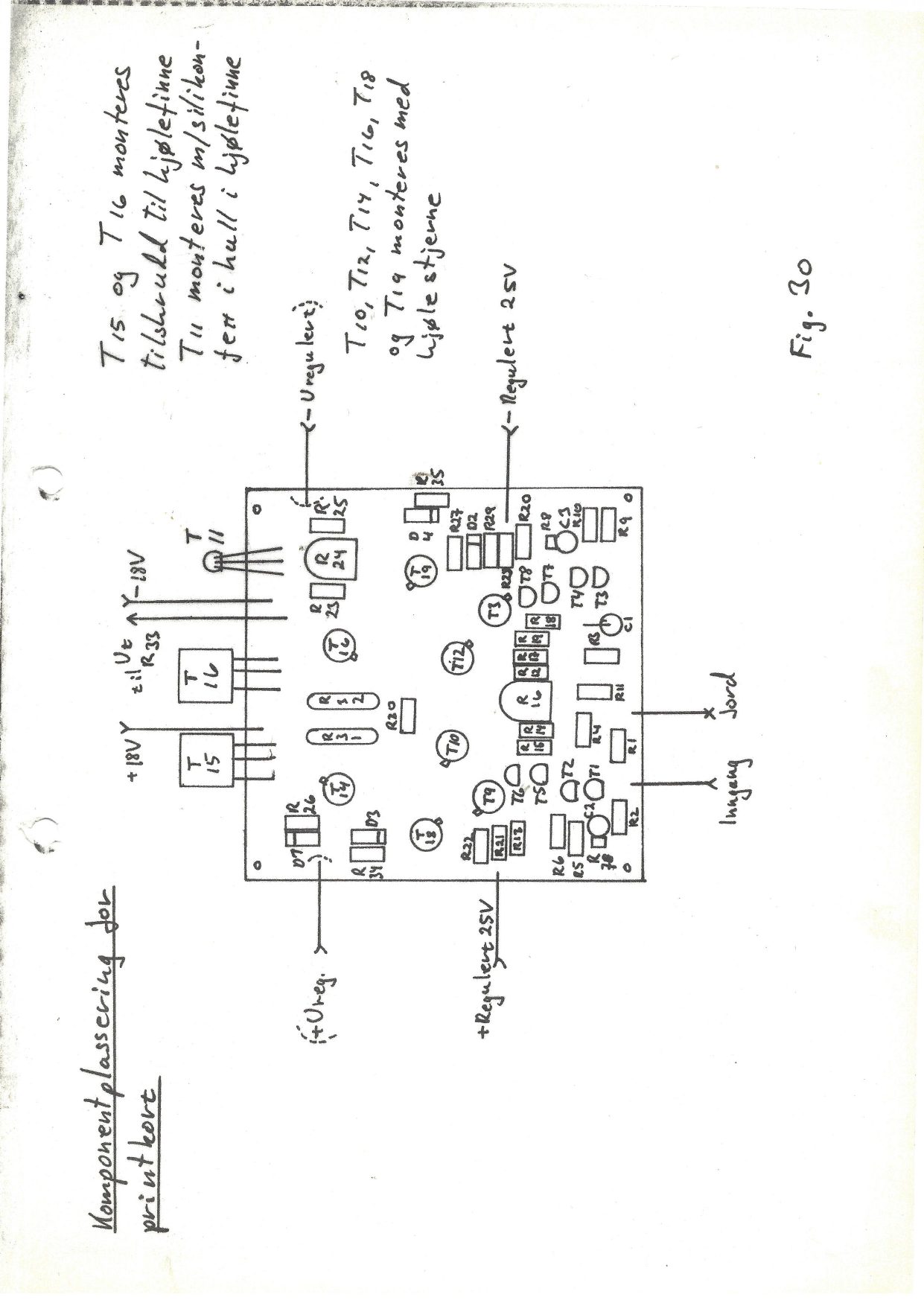
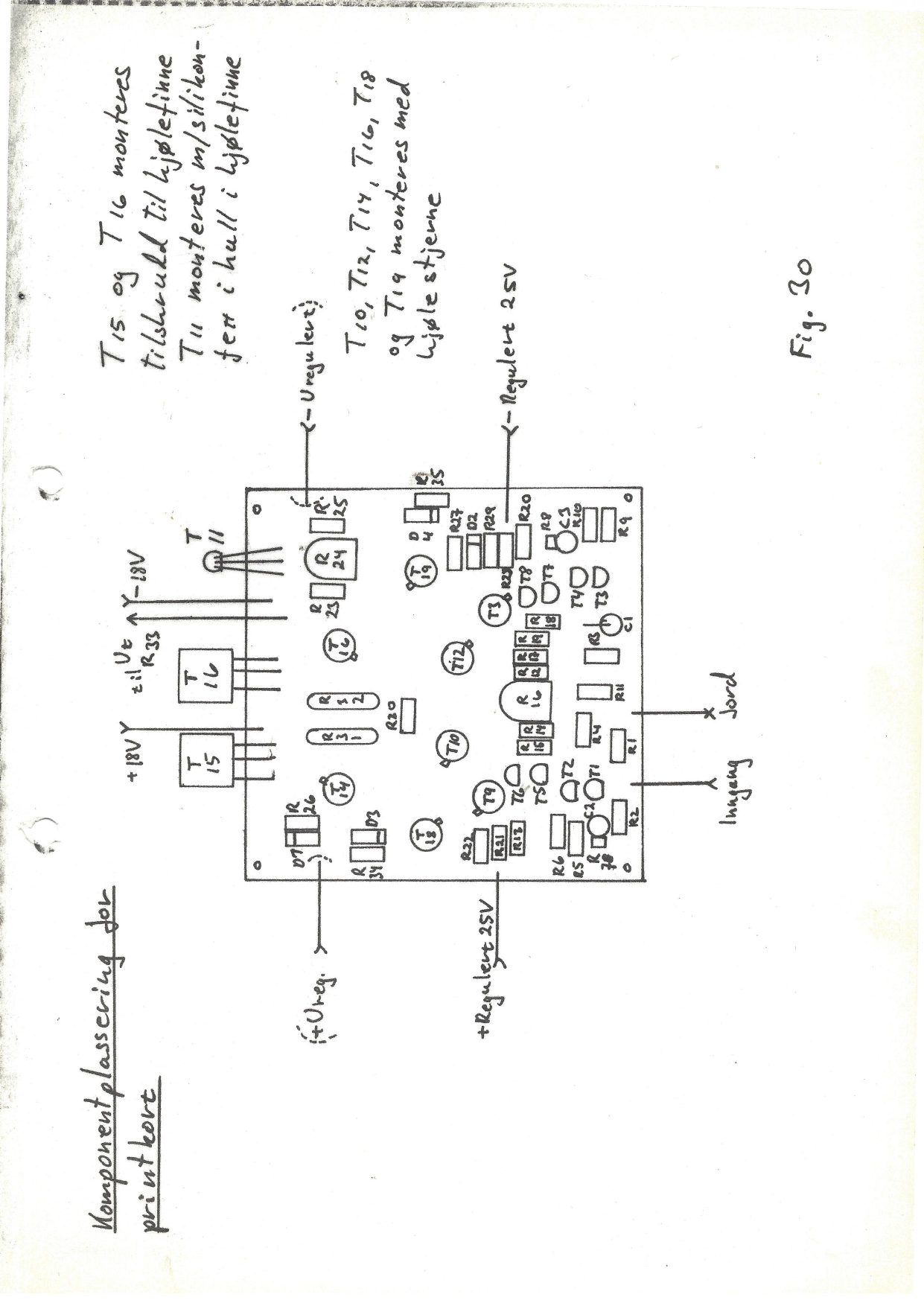
Oppgavens del II, oppkopling av print, er vist i fig. 30. Selve forsterkeren
er montert på en chassisplate med felles kjølefinne for begge kanaler montert
i bakkant. Kretskortene er festet med avstandsstykker til chassisplaten. Alle
tilkoplingene til printkortet er ført ut til en klemrekke som er montert på
framsiden av chassisplaten. Strømforsyningsledningene er da felles for begge
kanalene, mens jordtilkoplingene er separate.
Under målsettingen har vi nevnt undersøkelse av betydningen av komplementær
driving av utgangstransistorene mhp. linearitet, og betydningen av
spenningsstyring av utg. transistorene er teoretisk behandlet på sidene 7 til
12, blant analysen av utgangstrinnet. Kommentarer til de samme temaene er
også spredt rundt hele rapporten. Kommentarer også spesielt på dette i del
III, om betydningen av dette for det endelige resultatet.
Arbeidet med forsterkeren, og spesielt skriving av denne rapporten har tatt
lengre tid enn vi hadde regnet med til å begynne med. Vi har derfor ikke fått
med så mange måleresultater som vi hadde ønsket. Tendensen i de målingene vi
har foretatt er imidlertid så positive at oppgavens målsettinger må anses som
innfridd.
Del I — Teori og design
Målsetting
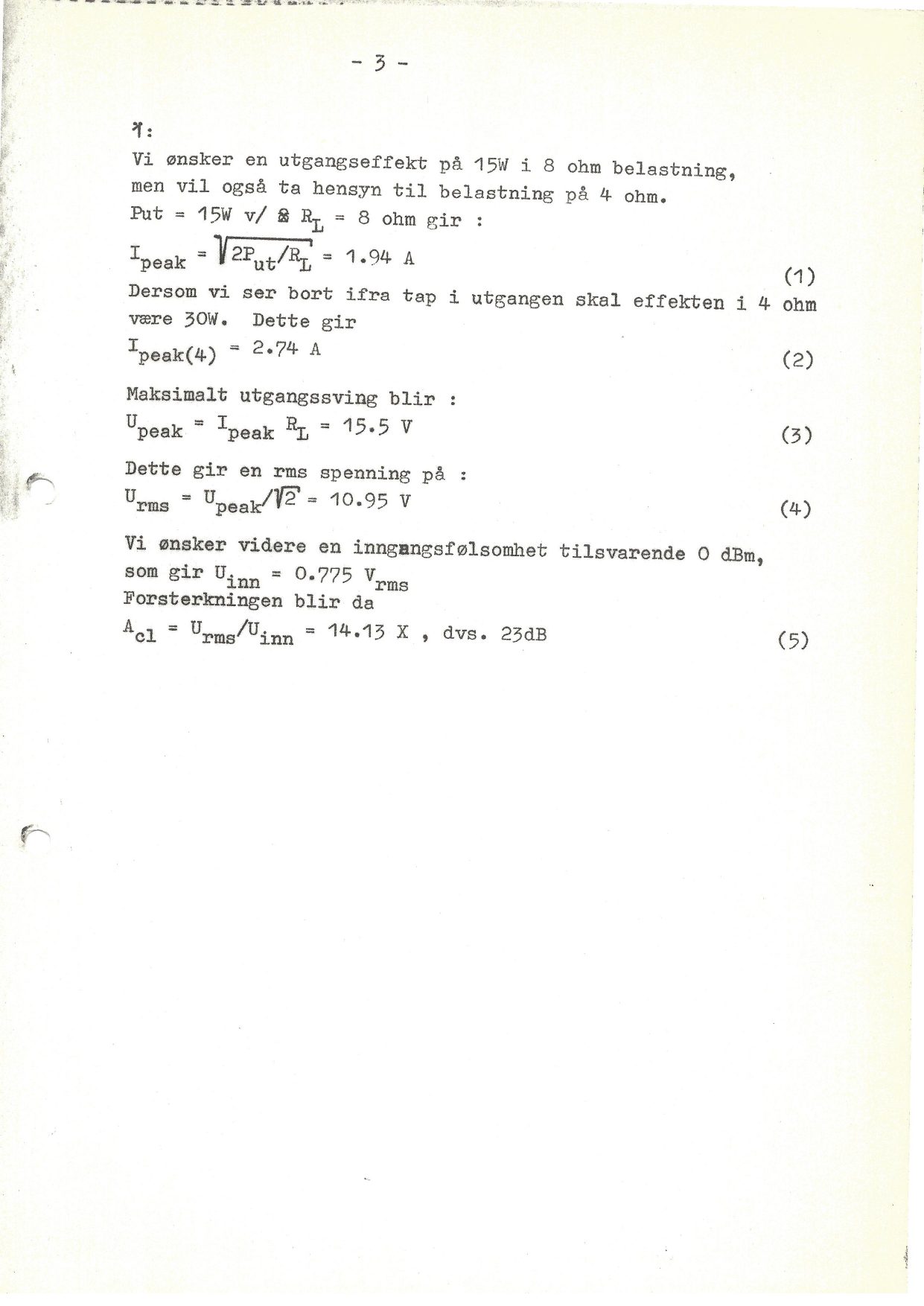
Vi ønsker en utgangseffekt på 15W i 8 ohm belastning, men vil også ta hensyn
til belastning på 4 ohm.
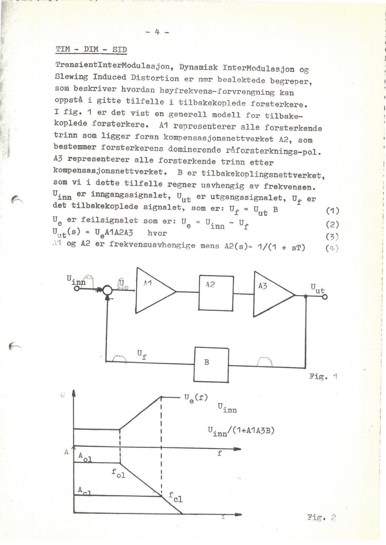
TransientInterModulasjon, Dynamisk InterModulasjon og Slewing Induced
Distortion er nær beslektede begreper, som beskriver hvordan
høyfrekvens-forvrengning kan oppstå i gitte tilfelle i tilbakekoplede
forsterkere.
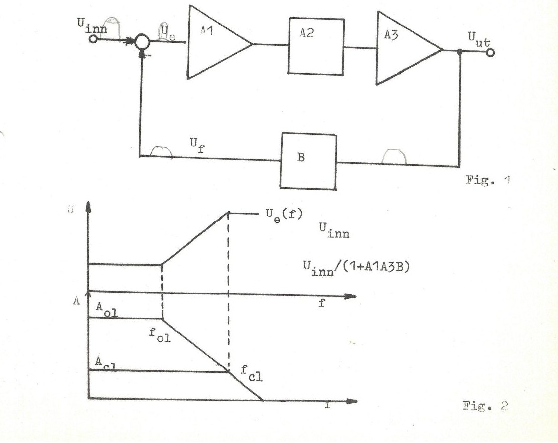
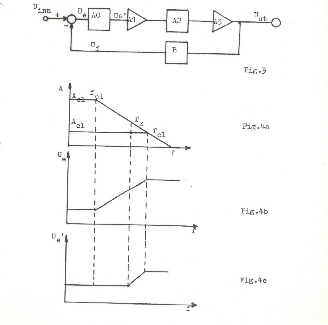
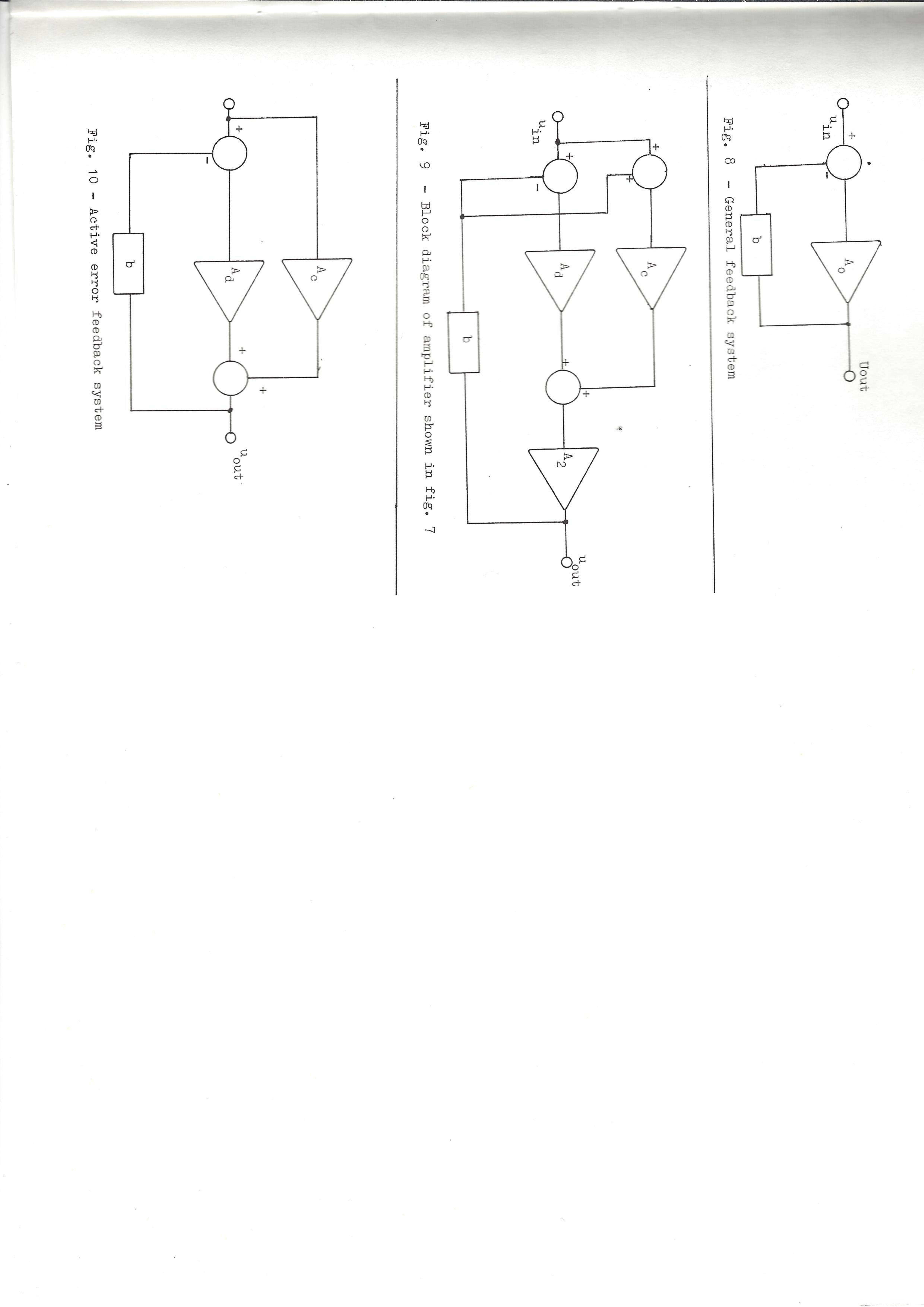
I fig. 1 er det vist en generell modell for tilbakekoplede forsterkere. A1
representerer alle forsterkende trinn som ligger foran kompensasjonsnettverket
A2, som bestemmer forsterkerens dominerende råforsterknings-pol. A3
representerer alle forsterkende trinn etter kompensasjonsnettverket. B er
tilbakekoplingsnettverket, som vi i dette tilfelle regner uavhengig av
frekvensen.
$U_{inn}$ er inngangssignalet, $U_{ut}$ er utgangssignalet, $U_f$ er det
tilbakekoplede signalet, som er: $U_f = U_{ut} B \tag{1}$
$U_e$ er feilsignalet som er: $U_e = U_{inn} - U_f \tag{2}$
$U_{ut}(s) = U_e A_1 A_2 A_3$ hvor $\tag{3}$
A1 og A2 er frekvensuavhengige mens $A_2(s) = 1/(1+sT) \tag{4}$
fol og kompensasjon
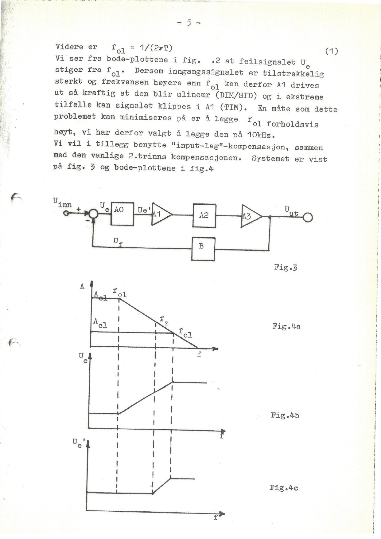
Videre er $f_{ol} = 1/(2\pi T) \tag{1}$
Vi ser fra bode-plottene i fig. 2 at feilsignalet $U_e$ stiger fra $f_{ol}$.
Dersom inngangssignalet er tilstrekkelig sterkt og frekvensen høyere enn
$f_{ol}$ kan derfor A1 drives ut så kraftig at den blir ulineær (DIM/SID) og i
ekstreme tilfelle kan signalet klippes i A1 (TIM). En måte som dette
problemet kan minimiseres på er å legge $f_{ol}$ forholdsvis høyt, vi har
derfor valgt å legge den på 10kHz.
Vi vil i tillegg benytte “input-lag”-kompensasjon, sammen med den vanlige
2.trinns kompensasjonen. Systemet er vist på fig. 3 og bode-plottene i fig.4
Dette gjør at inngangstrinnet ikke blir drevet hardere ut i området mellom
$f_{ol}$ og $f_z$. Ved å legge $f_z$ høyere enn den høyeste mulige
inngangsfrekvens, burde mulighetene for DIM/SID være minimale.
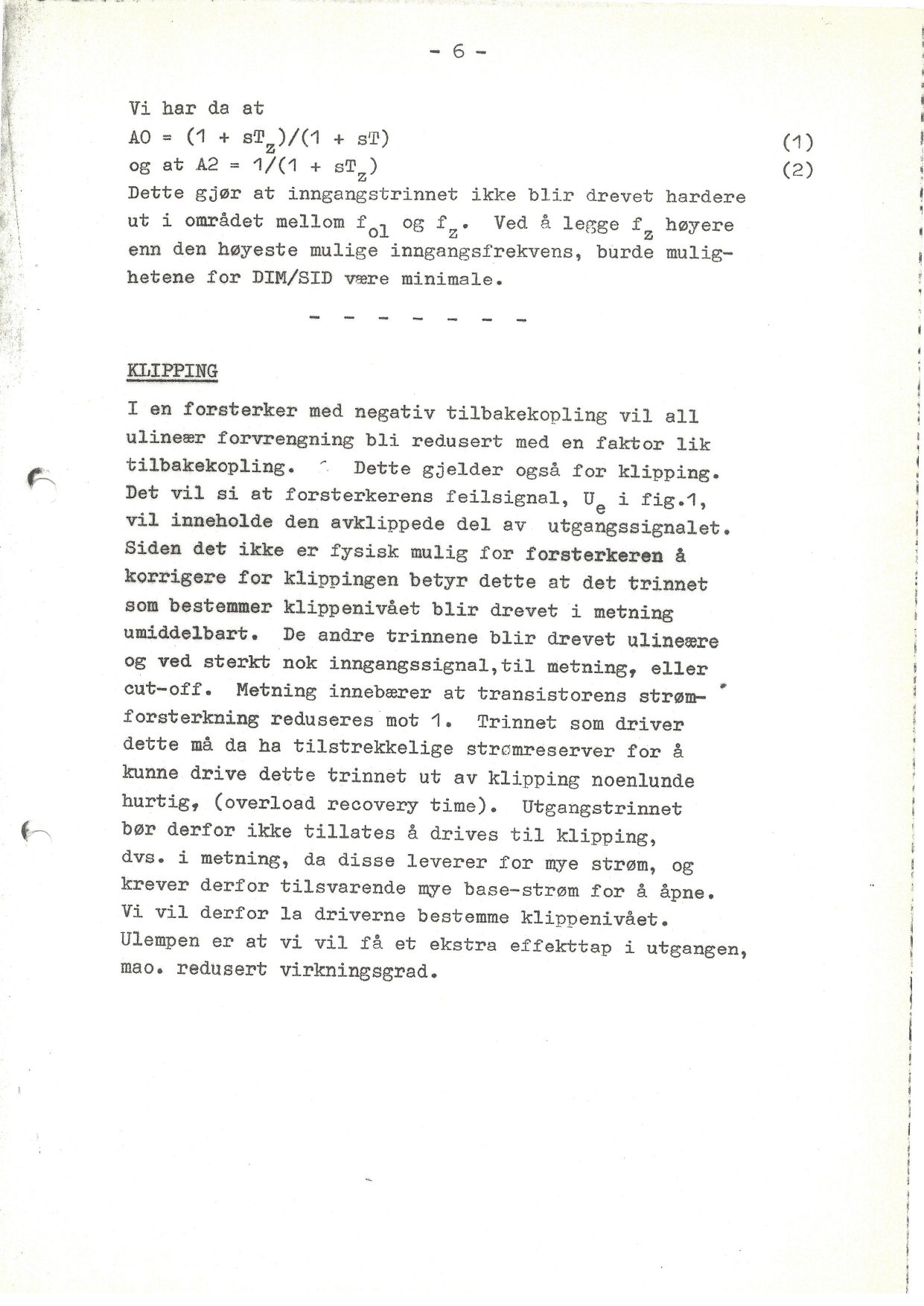
Klipping
I en forsterker med negativ tilbakekopling vil all ulineær forvrengning bli
redusert med en faktor lik tilbakekopling. Dette gjelder også for klipping.
Det vil si at forsterkerens feilsignal, $U_e$ i fig.1, vil inneholde den
avklippede del av utgangssignalet. Siden det ikke er fysisk mulig for
forsterkeren å korrigere for klippingen betyr dette at det trinnet som
bestemmer klippenivået blir drevet i metning umiddelbart. De andre trinnene
blir drevet ulineære og ved sterkt nok inngangssignal, til metning, eller
cut-off. Metning innebærer at transistorens strømforsterkning reduseres mot
Trinnet som driver dette må da ha tilstrekkelige strømreserver for å kunne
drive dette trinnet ut av klipping noenlunde hurtig, (overload recovery
time). Utgangstrinnet bør derfor ikke tillates å drives til klipping, dvs. i
metning, da disse leverer for mye strøm, og krever derfor tilsvarende mye
base-strøm for å åpne. Vi vil derfor la driverne bestemme klippenivået.
Ulempen er at vi vil få et ekstra effekttap i utgangen, mao. redusert
virkningsgrad.
Utgangstrinnet
Utgangstrinnet må kunne arbeide ved meget høye frekvenser. Dette gir at
utg.tr. må spenningsstyres, dvs. drives fra en lav impedans,
$Z_g \ll Z_{inn}$. Dette gir at emitterfølgeren får en grensefrekvens nærmere
$f_\alpha$ enn $f_\beta$.
For å få en enkel montering ønsker vi å benytte TO-39 kanner som drivere, med
evt. kjølestjerne. TO-39 transistorer har typisk $P_{c,maks} = 3W$ ved
$T_c = 25°C$, og en $\theta_{jc} = 60°C/W$, $T_{j,maks} = 200°C$.
En standard kjølestjerne for TO-39 har typ. $\theta_{sa} = 50°C/W$. Maks.
omgivelsestemperatur regnes vanligvis til $50°C$. Vi får da at:
når vi antar $\theta_{cs} \ll \theta_{jc} + \theta_{sa}$
Vi regner foreløpig med at forsterkningen i utg.trinnet er tilnærmelsesvis lik
1, og vi får da at $U_{CE}$ for driverne må være lik $U_{peak}$, dvs. 15.5V
(likn. 3.3). Dette gir absolutt maksimal strøm:
Av linearitetshensyn vil vi ha at hvilestrømmen i trinnet skal være vesentlig
større enn maksimal laststrøm. (Dette er nærmere forklart senere). Dette gir
at vi kan regne $I_C$ lik konstant.
SOAR kurvene for en typ. TO-39 (2N2219) og likn.3 gir oss en
$I_{C,maks} = 55$mA før second breakdown. Strømmen $I_C$ som velges bør
heller ikke være så stor at utgangstransistorene kan drives over sin
$I_{C,maks}$.
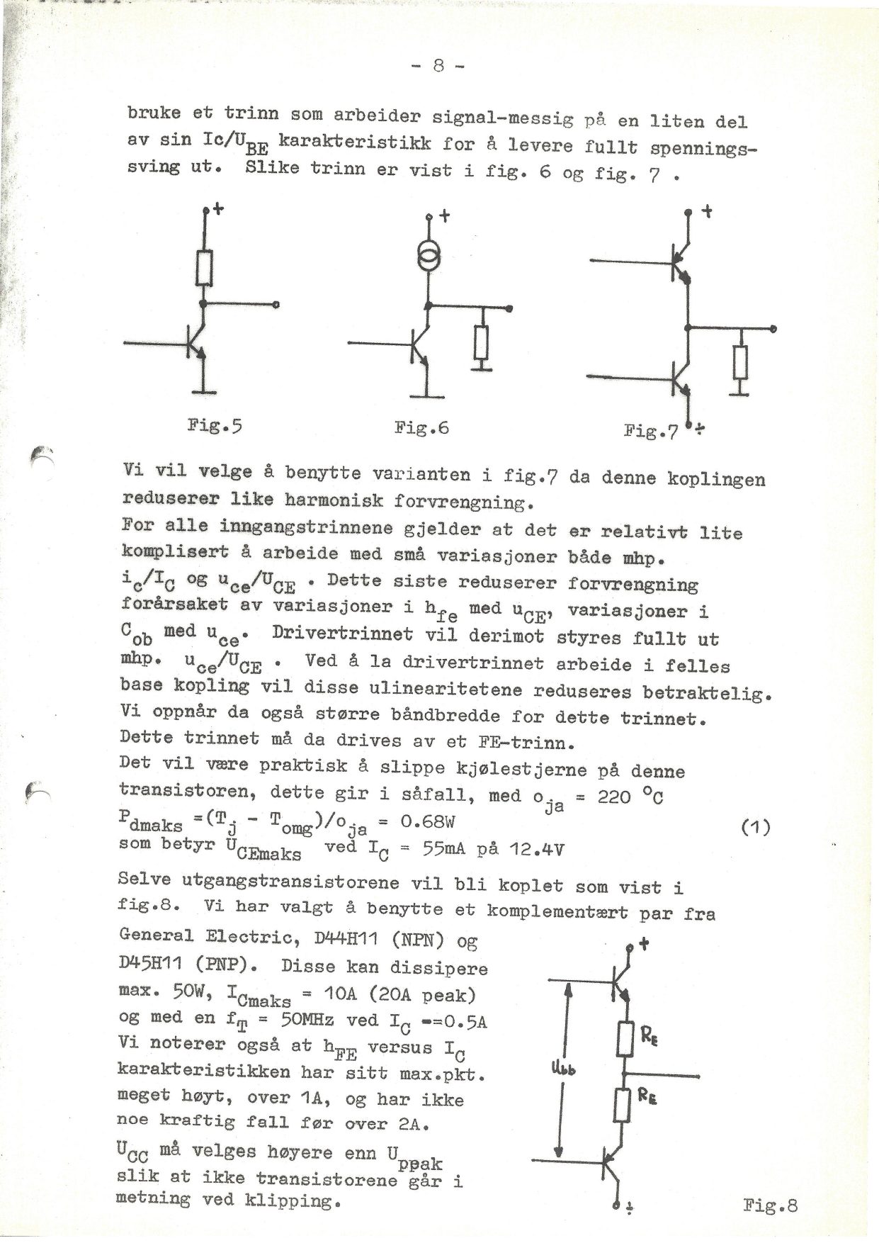
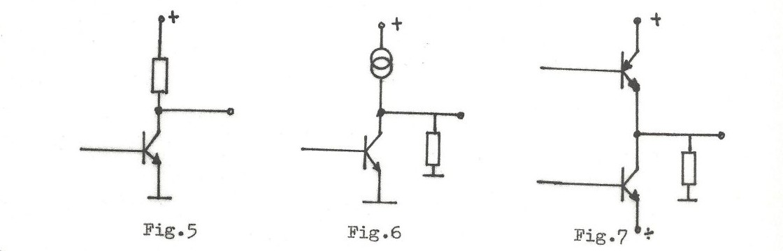
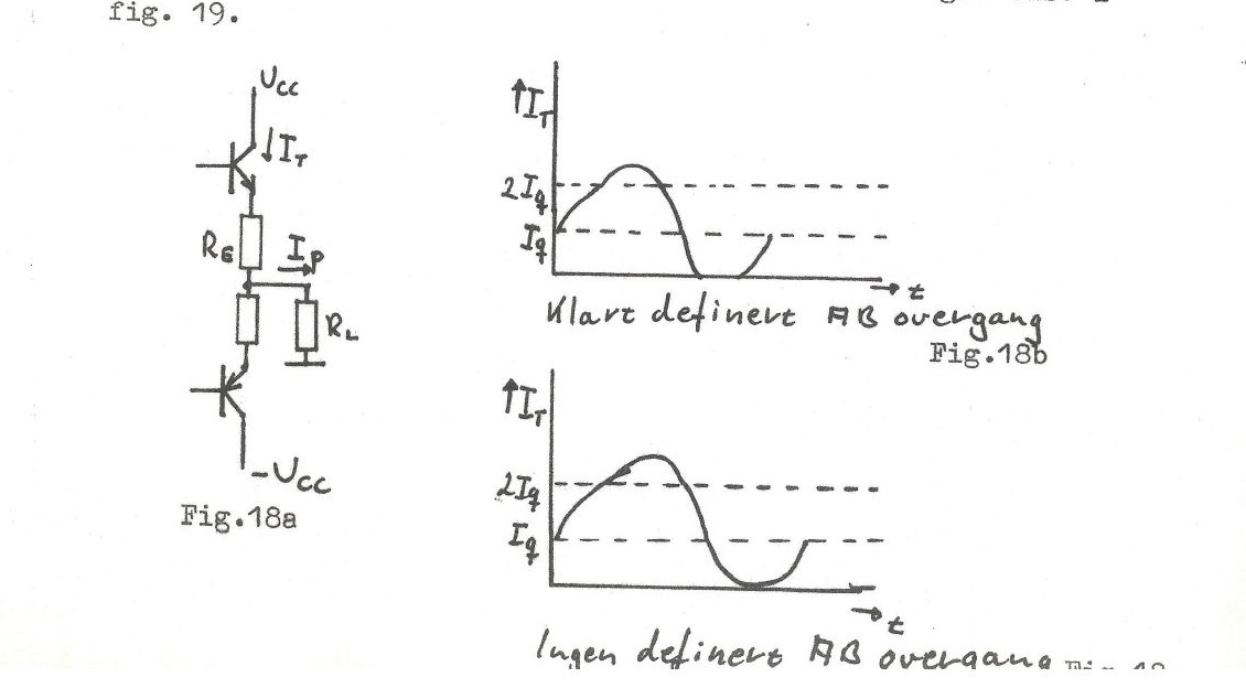
Et standard FE-koplet trinn (fig. 5) kan karakteriseres ved at trinnet må
doble sin strøm i forhold til hvilestrømmen, og redusere den samme til nær
null for å få fullt spenningssving på utgangen. Ved full utstyring vil
trinnet bli veldig ulineært. Dette ser en ved å betrakte $I_C$ versus $U_{BE}$
karakteristikken. For å få lav forvrengning bør en derfor
bruke et trinn som arbeider signal-messig på en liten del av sin
$I_c/U_{BE}$ karakteristikk for å levere fullt spenningssving ut. Slike trinn
er vist i fig. 6 og fig. 7.
Vi vil velge å benytte varianten i fig.7 da denne koplingen reduserer like
harmonisk forvrengning.
For alle inngangstrinnene gjelder at det er relativt lite komplisert å
arbeide med små variasjoner både mhp. $i_c/I_C$ og $u_{ce}/U_{CE}$. Dette
siste reduserer forvrengning forårsaket av variasjoner i $h_{fe}$ med
$u_{CE}$, variasjoner i $C_{ob}$ med $u_{ce}$. Drivertrinnet vil derimot
styres fullt ut mhp. $u_{ce}/U_{CE}$. Ved å la drivertrinnet arbeide i felles
base kopling vil disse ulineariteten reduseres betraktelig. Vi oppnår da også
større båndbredde for dette trinnet. Dette trinnet må da drives av et
FE-trinn.
Det vil være praktisk å slippe kjølestjerne på denne transistoren, dette gir
i såfall, med $\theta_{ja} = 220°C$:
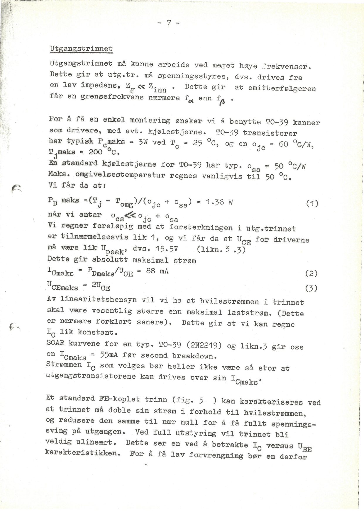
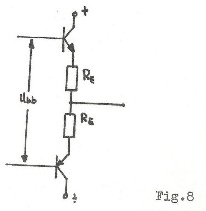
Selve utgangstransistorene vil bli koplet som vist i fig.8. Vi har valgt å
benytte et komplementært par fra General Electric, D44H11 (NPN) og D45H11
(PNP). Disse kan dissipere max. 50W, $I_{C,maks} = 10A$ (20A peak) og med en
$f_T = 50$MHz ved $I_C = 0.5A$. Vi noterer også at $h_{FE}$ versus $I_C$
karakteristikken har sitt max.pkt. meget høyt, over 1A, og har ikke noe
kraftig fall før over 2A.
$U_{CC}$ må velges høyere enn $U_{peak}$ slik at ikke transistorene går i
metning ved klipping.
Vi vil benytte ca. ±18V. Fra SOAR-kurvene ser vi da at maksimal hvilestrøm
$I_{Cq} = .35$A.
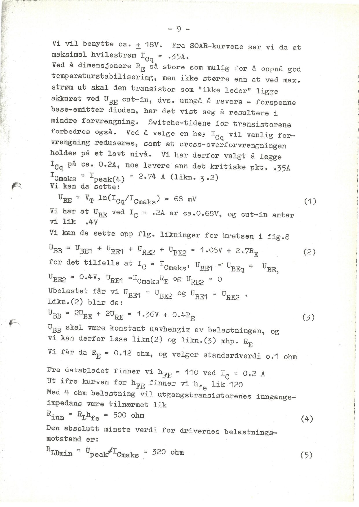
Ved å dimensjonere $R_E$ så store som mulig for å oppnå god
temperaturstabilisering, men ikke større enn at ved max. strøm ut skal den
transistor som “ikke leder” ligge akkurat ved $U_{BE}$ cut-in, dvs. unngå å
revers-forspenne base-emitter dioden, har det vist seg å resultere i mindre
forvrengning. Switche-tidene for transistorene forbedres også. Ved å velge en
høy $I_{Cq}$ vil vanlig forvrengning reduseres, samt at
cross-over-forvrengningen holdes på et lavt nivå. Vi har derfor valgt å legge
$I_{Cq}$ på ca. 0.2A, noe lavere enn det kritiske pkt. .35A
$$I_{C,maks} = I_{peak(4)} = 2.74\text{ A (likn. 3.2)} \tag{}$$
$U_{BB}$ skal være konstant uavhengig av belastningen, og vi kan derfor løse
likn(2) og likn.(3) mhp. $R_E$. Vi får da $R_E = 0.12$ ohm, og velger
standardverdi 0.1 ohm.
Fra databladet finner vi $h_{FE} = 110$ ved $I_C = 0.2$ A. Ut ifra kurven for
$h_{FE}$ finner vi $h_{fe}$ lik 120. Med 4 ohm belastning vil
utgangstransistorenes inngangsimpedans være tilnærmet lik:
$$R_{inn} = R_L h_{fe} = 500\text{ ohm} \tag{4}$$
Den absolutt minste verdi for drivernes belastningsmotstand er:
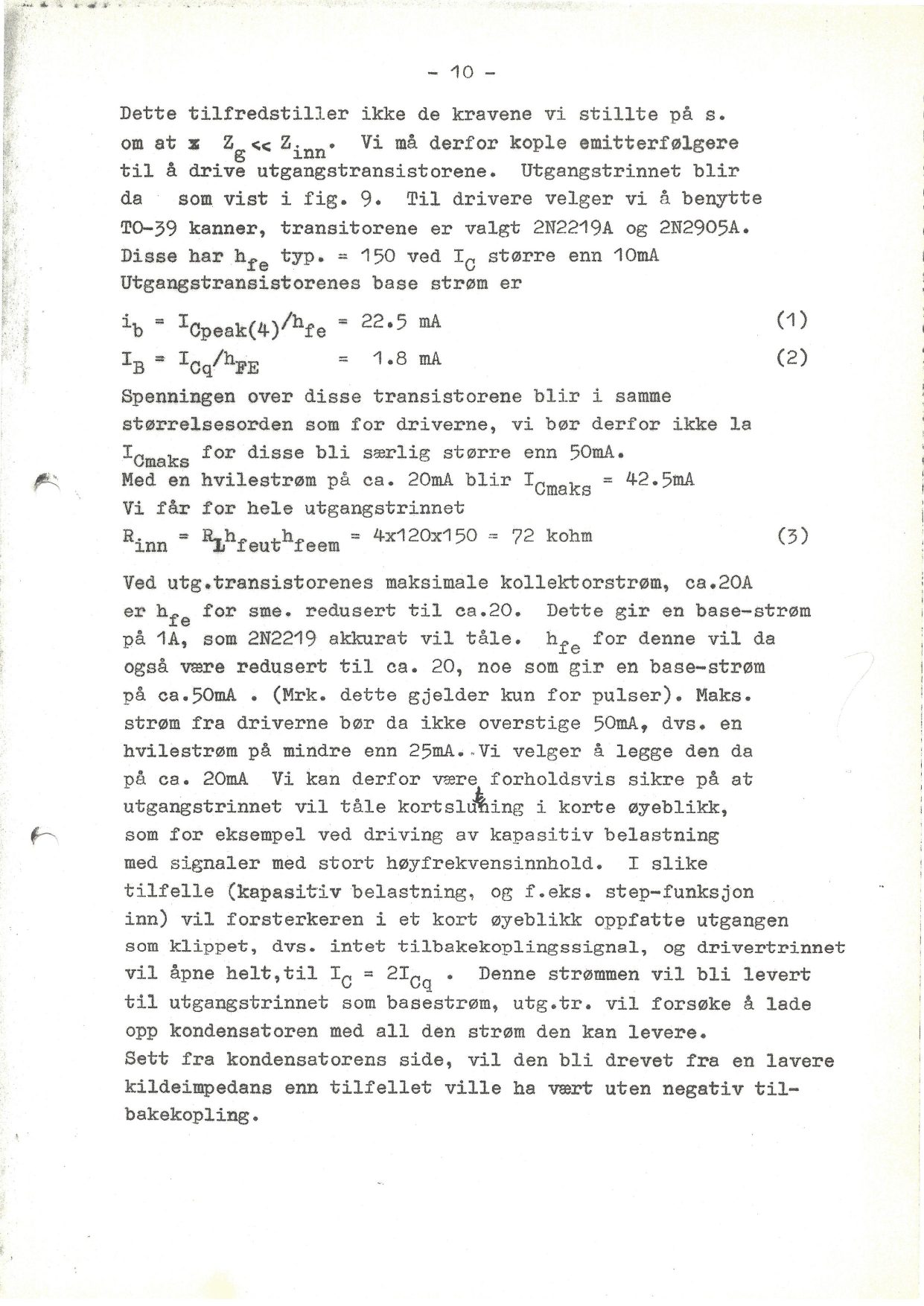
Dette tilfredstiller ikke de kravene vi stillte på s. om at
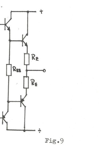
$Z_g \ll Z_{inn}$. Vi må derfor kople emitterfølgere til å drive
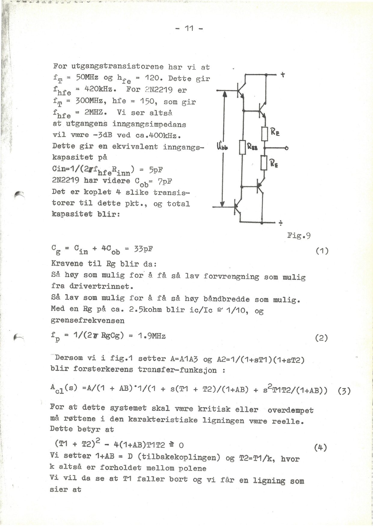
utgangstransistorene. Utgangstrinnet blir da som vist i fig. 9. Til drivere
velger vi å benytte TO-39 kanner, transitorene er valgt 2N2219A og 2N2905A.
Disse har $h_{fe}$ typ. = 150 ved $I_C$ større enn 10mA.
Spenningen over disse transistorene blir i samme størrelsesorden som for
driverne, vi bør derfor ikke la $I_{C,maks}$ for disse bli særlig større enn
50mA. Med en hvilestrøm på ca. 20mA blir $I_{C,maks} = 42.5$mA.
Ved utg.transistorenes maksimale kollektorstrøm, ca.20A er $h_{fe}$ for sme.
redusert til ca.20. Dette gir en basestrøm på 1A, som 2N2219 akkurat vil
tåle. $h_{fe}$ for denne vil da også være redusert til ca. 20, noe som gir
en base-strøm på ca.50mA. (Mrk. dette gjelder kun for pulser). Maks. strøm
fra driverne bør da ikke overstige 50mA, dvs. en hvilestrøm på mindre enn
25mA. Vi velger å legge den da på ca. 20mA. Vi kan derfor være forholdsvis
sikre på at utgangstrinnet vil tåle kortslutning i korte øyeblikk, som for
eksempel ved driving av kapasitiv belastning med signaler med stort
høyfrekvensinnhold. I slike tilfelle (kapasitiv belastning, og f.eks.
step-funksjon inn) vil forsterkeren i et kort øyeblikk oppfatte utgangen som
klippet, dvs. intet tilbakekoplingssignal, og drivertrinnet vil åpne
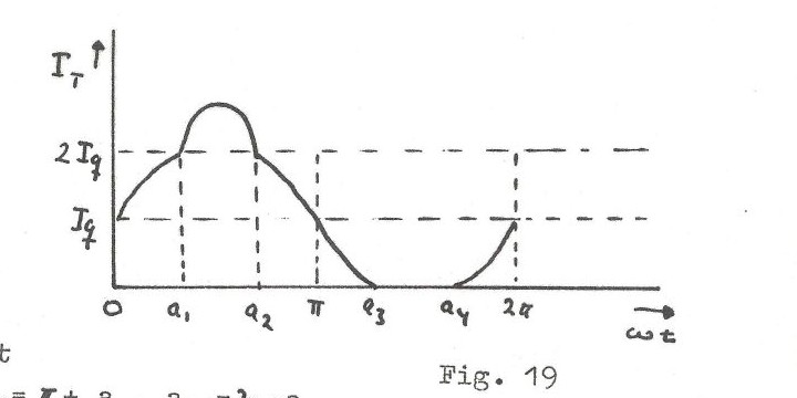
helt,til $I_C = 2I_{Cq}$. Denne strømmen vil bli levert til utgangstrinnet som
basestrøm, utg.tr. vil forsøke å lade opp kondensatoren med all den strøm den
kan levere. Sett fra kondensatorens side, vil den bli drevet fra en lavere
kildeimpedans enn tilfellet ville ha vært uten negativ tilbakekopling.
For utgangstransistorene har vi at $f_T = 50$MHz og $h_{fe} = 120$. Dette gir
$f_{hfe} = 420$kHz. For 2N2219 er $f_T = 300$MHz, $h_{fe} = 150$, som gir
$f_{hfe} = 2$MHz. Vi ser altså at utgangens inngangsimpedans vil være -3dB
ved ca.400kHz.
2N2219 har videre $C_{ob} = 7$pF. Det er koplet 4 slike transistorer til dette
pkt., og total kapasitet blir:
$$C_g = C_{in} + 4C_{ob} = 33\text{ pF} \tag{1}$$
Kravene til $R_g$ blir da: så høy som mulig for å få så lav forvrengning som
mulig fra drivertrinnet. Så lav som mulig for å få så høy båndbredde som
mulig. Med en $R_g$ på ca. 2.5kohm blir $i_c/I_C \approx 1/10$, og
grensefrekvensen:
Vi setter $1+AB = D$ (tilbakekoplingen) og $T_2 = T_1/k$, hvor $k$ altså er
forholdet mellom polene. Vi vil da se at $T_1$ faller bort og vi får en
ligning som sier at
$$k^2 + k(1-4D) + 1 \gtrsim 0 \tag{1}$$
Vi antar at $k \gg 1$ og at $D \gg 1$, noe som vil være tilfelle i praksis. Vi
får da:
$$k - 4D \gtrsim 0 \text{ altså at } k \geq 4D \tag{2}$$
Vi har valgt å legge den dominerende pol på 10kHz, og vi har funnet en ny pol
på 1.9MHz, dette gir $k = 190$ og vi får da at $D \leq 47.5$ dvs. 33dB.
Likn.(11.5) gir at $A_{cl} = 14X$ og siden:
$$A_{ol} = A_{cl} D \leq 660\text{ X} \tag{3}$$
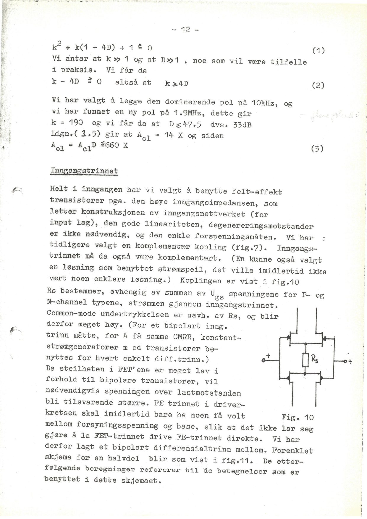
Inngangstrinnet
Helt i inngangen har vi valgt å benytte felt-effekt transistorer pga. den
høye inngangsimpedansen, som letter konstruksjonen av inngangsnettverket (for
input lag), den gode lineariteten, degenereringsmotstander er ikke
nødvendig, og den enkle forspenningsmåten. Vi har tidligere valgt en
komplementær kopling (fig.7). Inngangstrinnet må da også være komplementært.
(En kunne også valgt en løsning som benyttet strømspeil, det ville imidlertid
ikke vært noen enklere løsning.) Koplingen er vist i fig.10
$R_s$ bestemmer, avhengig av summen av $U_{gs}$ spenningene for P- og
N-channel typene, strømmen gjennom inngangstrinnet. Common-mode
undertrykkelsen er uavh. av $R_s$, og blir derfor meget høy. (For et
bipolart inng. trinn måtte, for å få samme CMRR, konstant-strømgeneratorer
med transistorer benyttes for hvert enkelt diff.trinn.)
Da steilheten i FET’ene er meget lav i forhold til bipolare transistorer, vil
nødvendigvis spenningen over lastmotstanden bli tilsvarende større. FE
trinnet i driverkretsen skal imidlertid bare ha noen få volt mellom
forsyningsspenning og base, slik at det ikke lar seg gjøre å la FET-trinnet
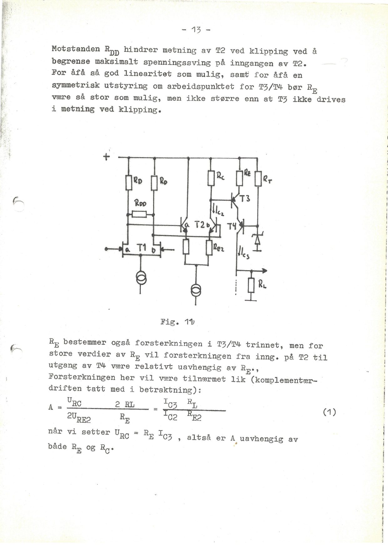
drive FE-trinnet direkte. Vi har derfor lagt et bipolart differensialtrinn
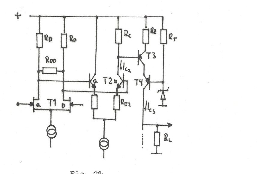
mellom. Forenklet skjema for en halvdel blir som vist i fig.11. De
etterfølgende beregninger refererer til de betegnelser som er benyttet i
dette skjemaet.
Motstanden $R_{DD}$ hindrer metning av T2 ved klipping ved å begrense
maksimalt spenningssving på inngangen av T2. For å få så god linearitet som
mulig, samt for å få en symmetrisk utstyring om arbeidspunktet for T3/T4 bør
$R_E$ være så stor som mulig, men ikke større enn at T3 ikke drives i metning
ved klipping.
$R_E$ bestemmer også forsterkningen i T3/T4 trinnet, men for store verdier av
$R_E$ vil forsterkningen fra inng. på T2 til utgang av T4 være relativt
uavhengig av $R_E$. Forsterkningen her vil være tilnærmet lik
(komplementærdriften tatt med i betraktning):
når vi setter $U_{RC} = R_E I_{C3}$, altså er A uavhengig av både $R_E$ og
$R_C$.
For utgangstransistorene har vi …(fortsetter side 14)
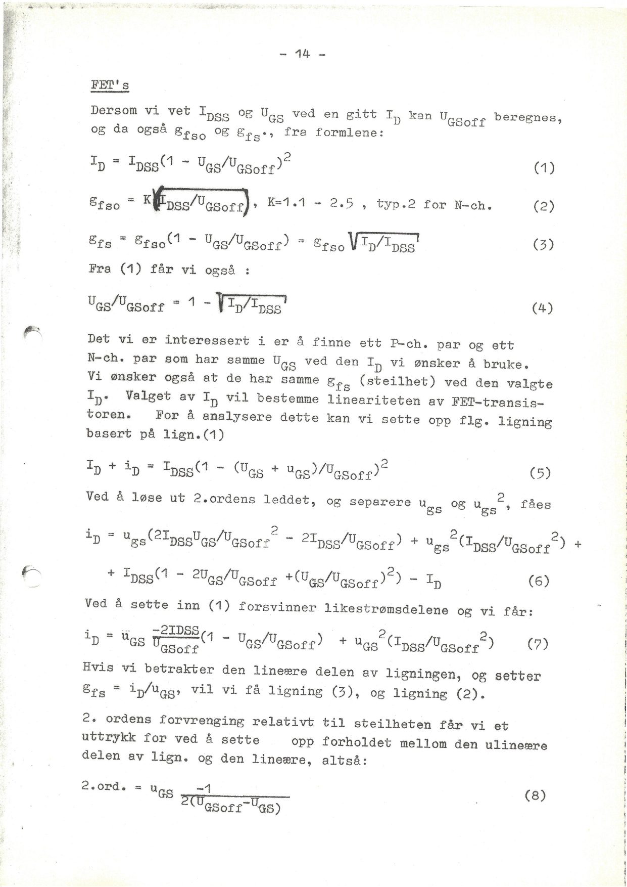
For å få lav forvrengning bør da $U_{GS} \ll U_{GSoff}$, og fra lign. (14.1)
gir dette høy $I_D$. Fra lign. (14.3) ser vi at dette også gir høy steilhet.
Drain-motstanden blir følgelig også lav, noe som gir høyere cut-off frekvens
på dette pkt.
Vi velger da å drive FET’ene på ca 1/3 $I_{DSS}$ slik at vi ved full
overstyring av inngangstrinnet akkurat ikke når $I_{DSS}$. Dersom vi antar
ingen mismatch mellom de 2 transistorene i hvert par vil alle like harmoniske
kanselleres.
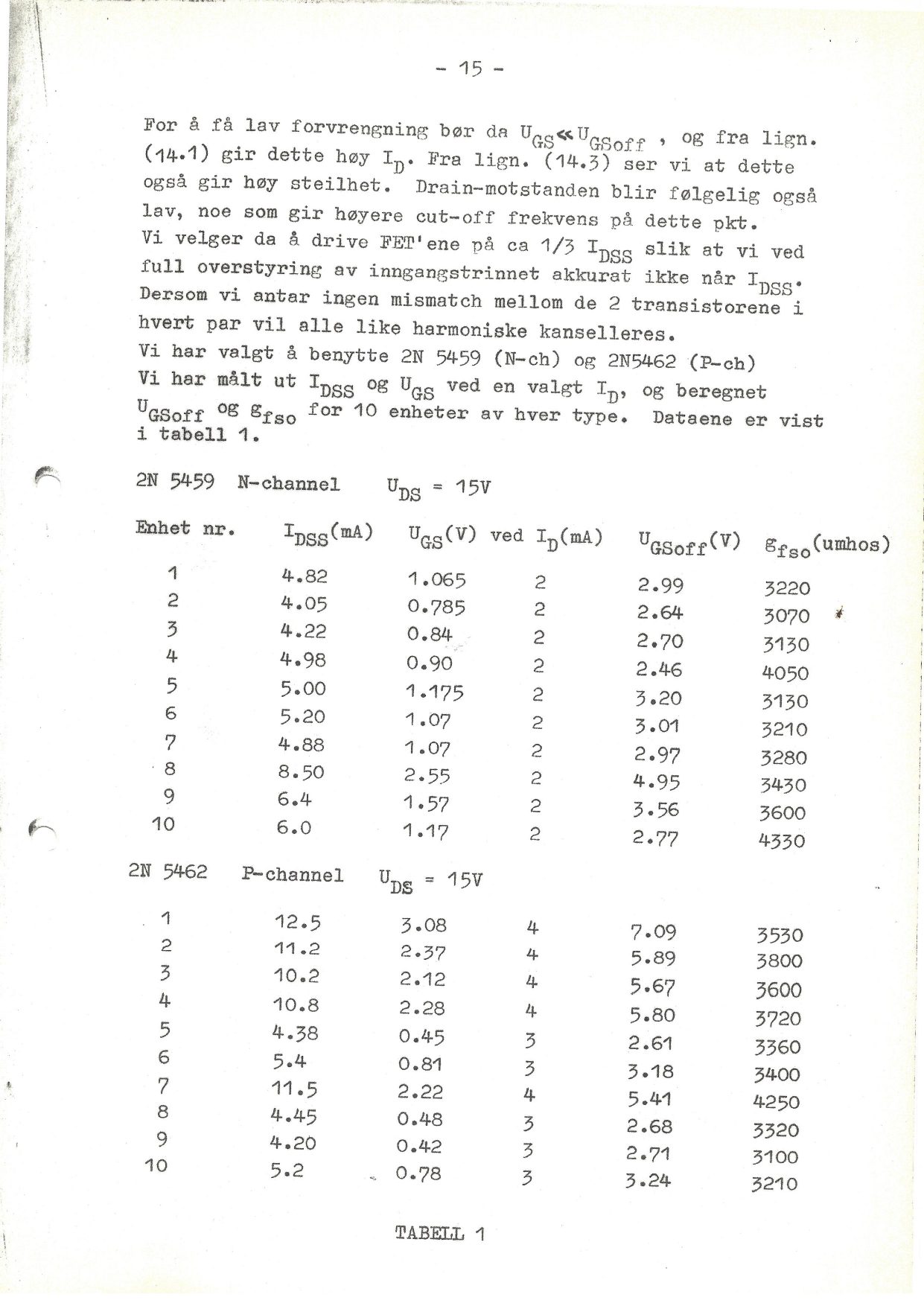
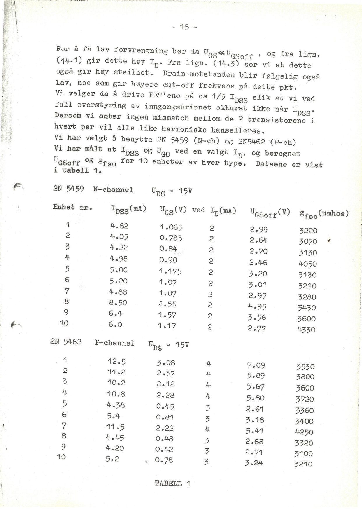
Vi har valgt å benytte 2N5459 (N-ch) og 2N5462 (P-ch). Vi har målt ut
$I_{DSS}$ og $U_{GS}$ ved en valgt $I_D$, og beregnet $U_{GSoff}$ og
$g_{fso}$ for 10 enheter av hver type. Dataene er vist i tabell 1.
Ut ifra dataene i tab.1 velger vi å benytte:
For kanal 1: N-ch. enh.nr 1 og 6, P-ch. enh. nr. 6 og 10
For kanal 2: N-ch. enh. nr 2 og 3, P-ch. enh. nr. 5 og 8
Disse har $I_{DSS}$ mellom 4 og 5mA, og vi velger da å drive dem på ca.
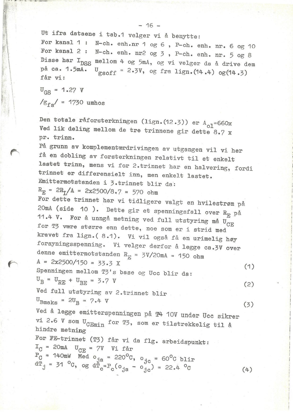
1.5mA. $U_{gsoff} = 2.3V$, og fra lign.(14.4) og(14.3) får vi:
Den totale råforsterkningen (lign.(12.3)) er $A_{ol}=660x$. Ved lik deling
mellom de tre trinnene gir dette 8.7 x pr. trinn.
På grunn av komplementærdrivingen av utgangen vil vi her få en dobling av
forsterkningen relativt til et enkelt lastet trinn, mens vi for 2.trinnet har
en halvering, fordi trinnet er differensielt inn, men enkelt lastet.
For dette trinnet har vi tidligere valgt en hvilestrøm på 20mA (side 10).
Dette gir et spenningsfall over $R_E$ på 11.4 V. For å unngå metning ved full
utstyring må $U_{CE}$ for T3 være større enn dette, noe som er i strid med
kravet fra lign.(8.1). Vi vil også få en urimelig høy forsyningsspenning. Vi
velger derfor å legge ca.3V over denne emittermotstanden:
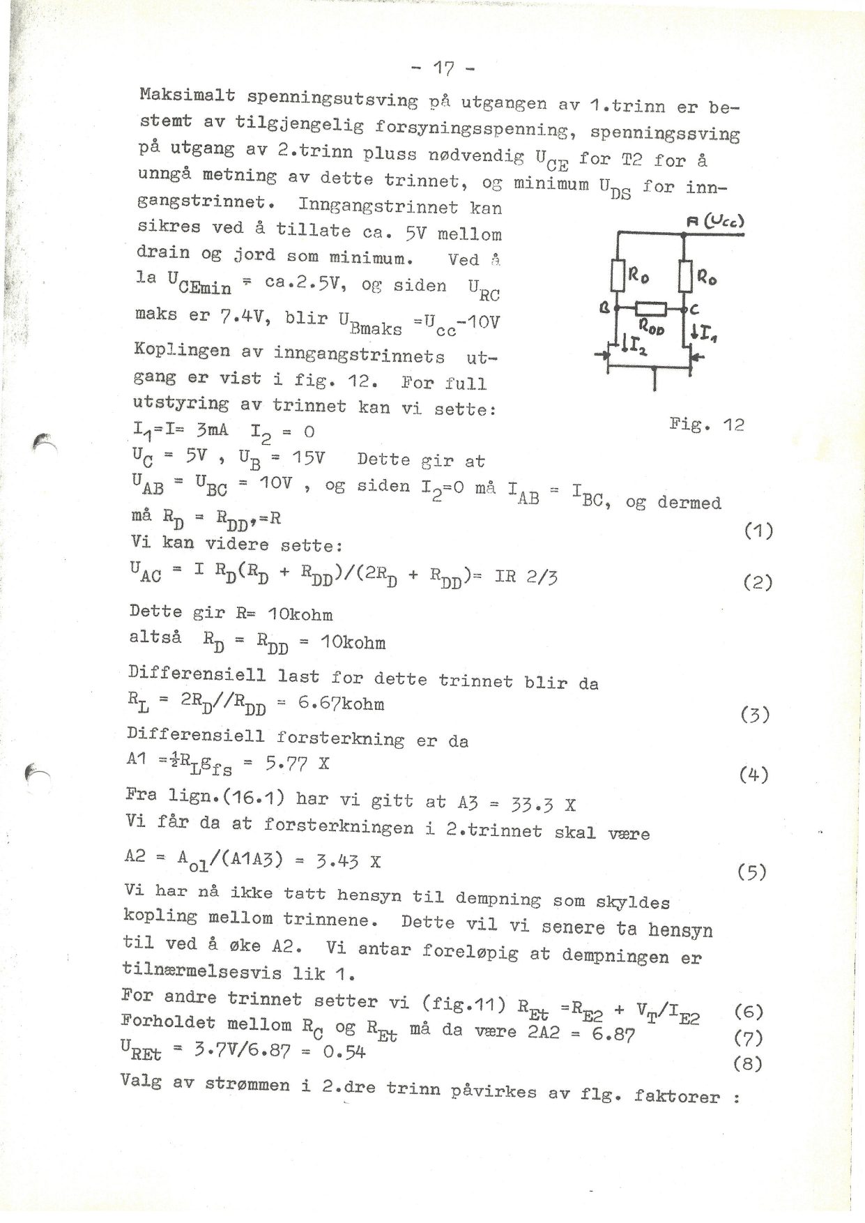
Maksimalt spenningsutsving på utgangen av 1.trinn er bestemt av tilgjengelig
forsyningsspenning, spenningssving på utgang av 2.trinn pluss nødvendig
$U_{CE}$ for T2 for å unngå metning av dette trinnet, og minimum $U_{DS}$ for
inngangstrinnet. Inngangstrinnet kan sikres ved å tillate ca. 5V mellom drain
og jord som minimum. Ved å la $U_{CEmin} = $ ca.2.5V, og siden $U_{RC}$ maks
er 7.4V, blir $U_{Bmaks} = U_{cc} - 10V$.
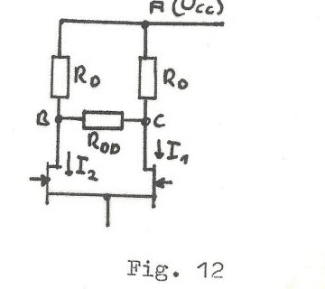
Koplingen av inngangstrinnets utgang er vist i fig. 12. For full utstyring av
trinnet kan vi sette: $I_1 = I = 3$mA, $I_2 = 0$; $U_C = 5V$, $U_B = 15V$.
Dette gir at $U_{AB} = U_{BC} = 10V$, og siden $I_2=0$ må $I_{AB} = I_{BC}$,
og dermed må $R_D = R_{DD} = R$.
$$U_{AC} = I R_D(R_D + R_{DD})/(2R_D + R_{DD}) = IR \cdot 2/3 \tag{2}$$
Dette gir $R = 10$kohm, altså $R_D = R_{DD} = 10$kohm.
Vi har nå ikke tatt hensyn til dempning som skyldes kopling mellom trinnene.
Dette vil vi senere ta hensyn til ved å øke $A_2$. Vi antar foreløpig at
dempningen er tilnærmelsesvis lik 1.
For andre trinnet setter vi (fig.11) $R_{Et} = R_{E2} + V_T/I_{E2} \tag{6}$
Forholdet mellom $R_C$ og $R_{Et}$ må da være $2A_2 = 6.87 \tag{7}$
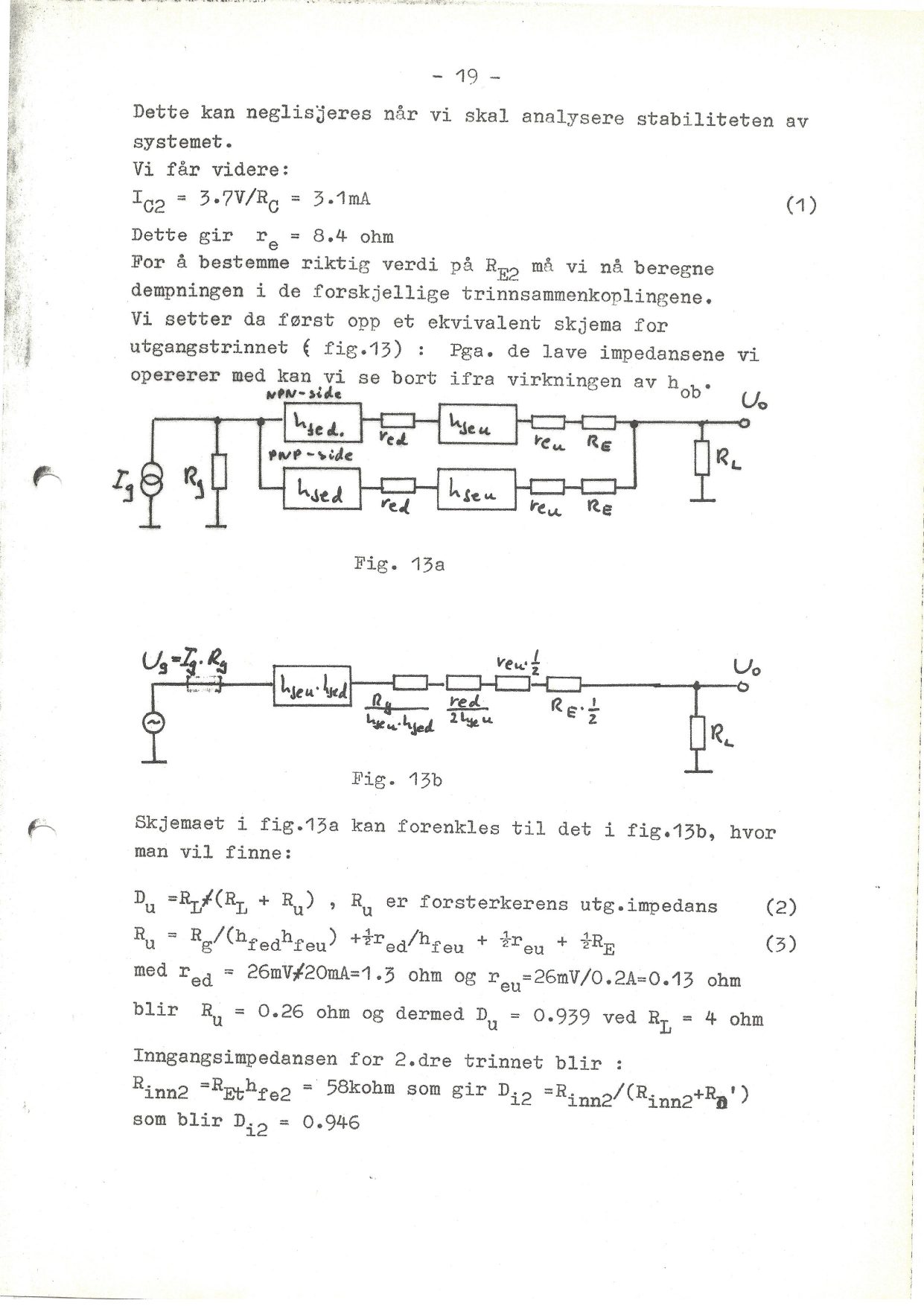
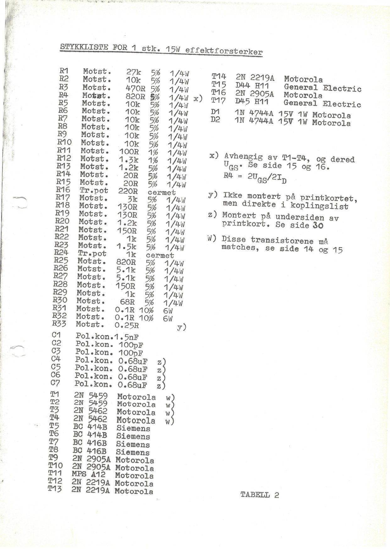
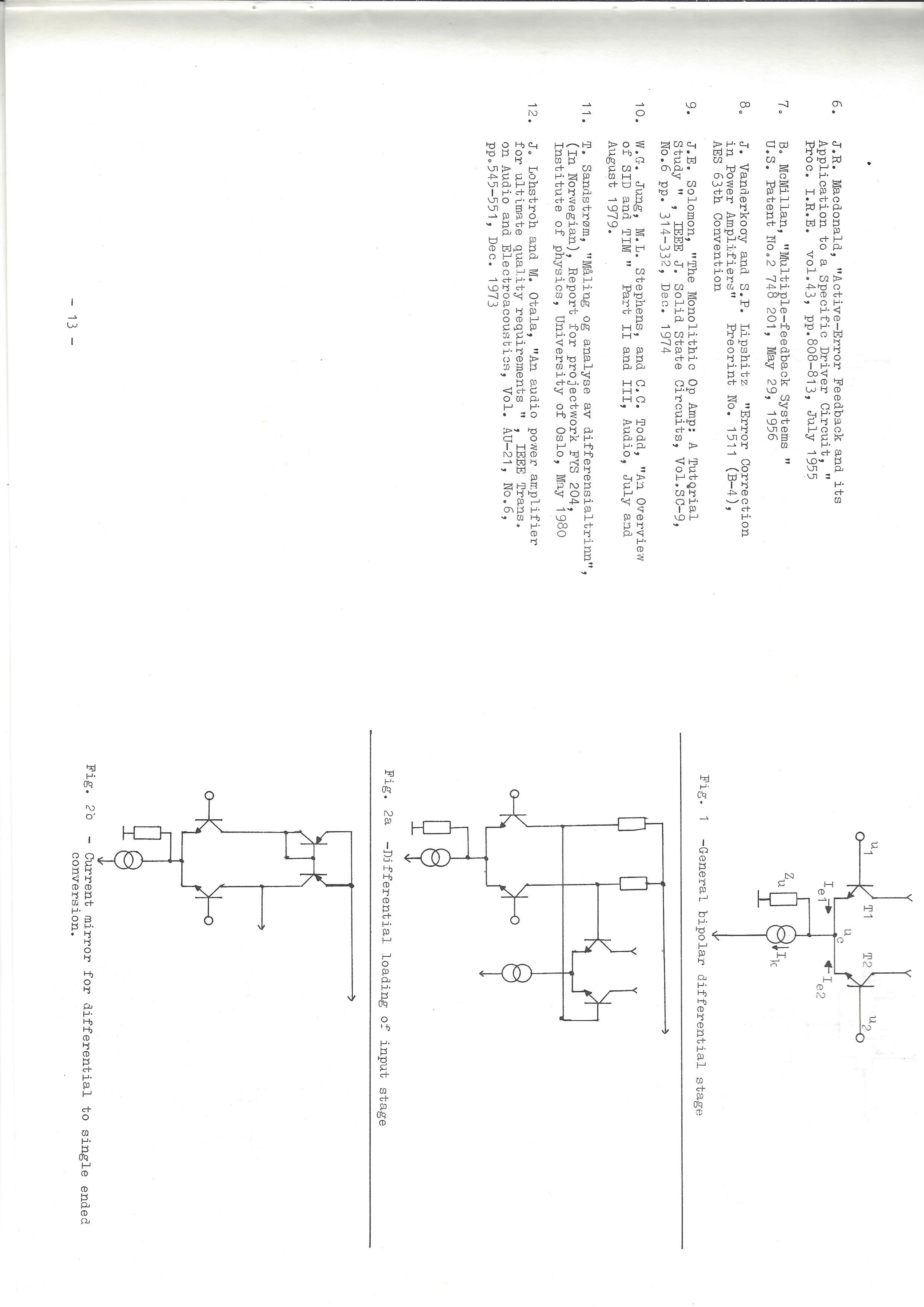
$$U_{REt} = 3.7\text{V}/6.87 = 0.54 \tag{8}$$
Valg av strømmen i 2.dre trinn påvirkes av flg. faktorer:
Høy strøm gir: Høy grensefrekvens mellom $R_L$ og tilhørende node-kapasitet.
Lav forvrengning pga. $h_{fe}$ ulineariteter i pkt. $R_L$-neste trinn, pga.
lav generatorimpedans for dette trinn.
Lav strøm gir: Lav forvrengning pga. $h_{fe}$ ulinearitet i pkt. $R_D$-2.trinn,
pga. av lav belastning av denne kildeimpedansen.
I dette tilfellet er ikke ulinearitet i $i_c$ versus $u_{BE}$ karakteristikken
noe problem, da trinnets utstyring er låst av kravene til utnivå fra hele
forsterkeren. Lign.(13.1) sier at $I_{C2}$ er omvendt proporsjonal med
$R_{E2}$ for konstant A. Ulineariteten er avhengig av forholdet mellom
$r_e = V_T/I_{C2}$ og $R_{E2}$, og av forholdet mellom $i_C/I_C$. Dette siste
er konstant pga. valget av virkningsgrad av 3.dje trinn. Ved å betrakte
systemet i fig.11, ser man at virkningsgraden av 2.re trinn er lik
virkningsgraden av 3dje trinn. Det andre forholdet, $r_e/R_{E2}$, blir også
konstant pga. kravet til forsterkning gitt i lign(13.1).
Inngangsimpedansen for 3.dje trinn med $h_{fe}$ for T3 lik 150 er:
Dersom vi regner $h_{fe}$ ulinearitet som like for 2.dre og 3.dje trinn,
uavhengig av hvor de arbeider på $h_{fe}$ versus $i_C$ karakteristikken, og
lar $h_{fe}$-forvrengningsbidraget fra hvert trinn være like, kan vi sette
graden av strømstyring like for trinnene, dvs:
Dette gir $r_e = 8.4$ ohm. For å bestemme riktig verdi på $R_{E2}$ må vi nå
beregne dempningen i de forskjellige trinnsammenkoplingene.
Vi setter da først opp et ekvivalent skjema for utgangstrinnet (fig.13): Pga.
de lave impedansene vi opererer med kan vi se bort ifra virkningen av
$h_{ob}$.
Skjemaet i fig.13a kan forenkles til det i fig.13b, hvor man vil finne:
Vi har valgt å benytte BC414 (NPN) og BC416(PNP) i 2.dre trinnet, og vi må da
benytte B-selektering for å tilfredstille kravet til $h_{fe}$.
Prinsipielt kan en serie-tilbakekoplet forsterker se ut som på fig.14.
Forsterkningen er da lik:
$$A_{cl} = A_{ol}/(1+A_{ol}B) \tag{6}$$
hvor $B = R_s/(R_s+R_f) \tag{7}$
Dette nettverket, (B), bør være så lavimpedant som mulig for å unngå
problemer med evt. kapasiteter på ÷ inngangen. Vi har at maks. utspenning er
15.5V, og det er praktisk å benytte 1/4W motstandere. Minste verdi for
$R_f + R_s$ blir da:
$$R = (15.5)^2/0.25 = 860\text{ ohm} \tag{}$$
Lign. 6 kan omformes til:
$$B = (A_{ol} - A_{cl})/(A_{ol}A_{cl}) \tag{8}$$
Med de verdier vi tidligere har funnet for $A_{ol}$ og $A_{cl}$ blir
$B = 72.5\times10^{-3}$. Lign. 7 kan omformes til:
$$R_s = R_f B/(1-B) \tag{}$$
Vi velger da $R_f = 1.3$kohm, og vil da få $R_s = 100$ ohm. (Fig. 14, se
side 20 over, viser det seriekoplede tilbakekoplingsnettverket.)
Siden det 2.dre trinnet er differensielt inn og enkelt lastet vil
transfer-karakteristikken ha 2 poler og ett nullpkt. Dersom vi antar at
trinnet drives fra to uavhengige generatorer med lik kildeimpedans, og hvis
generatorspenninger er i nøyaktig motfase, vil nullpunktet ligge en oktav
over første polpunkt.
Vi setter generatorimpedansen lik $R_D'$, for begge generatorer. Den
belastede delens inngangskapasitet er da:
$$C_i = C_{ob}(1+2A_2) \tag{1}$$
Med $C_{ob} = 5$pF, og $A_2=4.09$ blir $C_i = 46$pF. For den andre siden blir
$C_i = C_{ob} = 5$pF.
Første pol blir da på $f = 1$MHz, andre pol 9x høyere, og nullpkt. på ca.2MHz.
Ved å legge inn en kondensator tvers over den differensielle inngangen kan
virkningen av dette minimeres, og vi får da en fast cut-off frekvens lavere
ned. Ved å betrakte fig.3 og fig.4, ser man at denne cut-off-frekvensen er
kalt $f_z$.
Vi har valgt å benytte $C=100$pF, som gir en $f_z=239$kHz. Inngangsnettverket
$A_0$ skal da inneholde en pol på 10kHz og et nullpkt. på 239kHz. For å få en
definert pol på 10kHz legger vi en seriemotstand inn på inngangen.
Blokkskjematisk løsning er vist i fig. 15.
Nettverkets polpkt er:
$$f_p = 1/(2\pi C \cdot R_t), \quad R_t = R_i + R_f B + R_z \tag{2,3}$$
Nettverkets nullpkt: $f_n = 1/(2\pi C R_z) \tag{4}$
Vi får da $f_n/f_p = 23.9 = (R_i+R_f B+R_z)/R_z \tag{5}$
som gir $R_z = (R_i+R_f B)/(1-f_n/f_p) \tag{6}$
Vi velger $R_i = 10$kohm og får da $R_z = 440$ ohm, $C = 1.5$nF
Forspenningen av 2.dre trinnet er vist i fig.16. $U_D$ er drain-spenningen på
inngangstrinnet som er lik 10V i hvilestilling.
Spenningen over $R_K$ blir da: $U_{RK} = 2U_D - 2(U_{BE}+U_{RE}) = 18$V
Strømmen gjennom $R_K$ er lik $2I_{C2} = 2\times3.1$mA$=6.2$mA. $R_K$ blir da
3.0k.
I fig.9 er det markert at vi skal ha en viss forspenning $U'_{bb}$, av
utgangstrinnet. Dette for at transistorene skal forspennes til kl.AB drift. I
fig.17 er denne forspenningskretsen vist. Transistoren monteres slik at den
er i termisk kontakt med kjøleribben, og den vil dermed justere forspenningen
i takt med reduksjon/økning av utgangstransistorenes base-emitterspenninger
som funksjon av temperaturvariasjoner. Vi har valgt å benytte en
Darlington-transistor til dette (MPSA-12), slik at transistorens base-strøm
ikke skal påvirke forspenningen. Trimmepotensiometeret gjør at man kan
justere forspenningen til den ønskede tomgangstrøm i utgangen er oppnådd.
Potensiometeret er koplet slik at ved mekanisk svikt i viperen, dvs. viperen
mister kontakt med kullbanen, noe som lett kan skje med ikke-innkapslede
potensiometere ved mekanisk berøring, vil forspenningen synke, og dermed
tomgangsstrømmen reduseres, slik at ikke utgangen ødelegges.
$U_{BE}$ for Darlington-transistoren er regnet lik 1.2V. Nominell $U'_{bb}$
er lik $4\times0.65V = 2.6V$. Maksimal variasjon av $U'_{bb}$ valgt lik
±0.5V. Vi kan sette:
$$IR_2/2 = U_{var} = U_{BE} + U'_{bb} \tag{2}$$
Med $R_2$ lik 1kohm (mest/best tilgjengelige verdi) blir $I=923\mu A$
Vi har nevnt tidligere at utgangstrinnet må ha en høyere
forsyningsspenning enn “normalt”, for å unngå å gå i metning ved klipping. Vi
har derfor lagt $U_{cc}$ for utgangstrinnet på ±18V.
Vi har fra tidligere at hvilestrømmen $I_q=0.2$A. Vi har tidligere valgt å
benytte små verdier for emittermotstandene (s. 9). Dette gir at vi ikke vil
få en klart definert overgang mellom klasse A drift og klasse B drift.
Fig.18 b og c viser dette. Vi må likevel anta at vi har en definert overgang
for å kunne beregne effekttapet. Det virkelige effekttapet vil sannsynligvis
være noe større.
Så lenge forsterkeren arbeider i klasse A området vil utgangen fungere som to
parallell-koplede transistorer, det betyr at strømmen gjennom hver av dem er
halv-parten av strømmen gjennom lasten. Da det er komplementærdrift er det
absoluttverdien av strømmen gjennom transistorene som er like, og strømmene
er motsatt rettede.
I klasse B området vil transistorene vekselvis sperre og lede, slik at
strømmen gjennom hver av dem er lik strømmen gjennom lasten i lede-fasen.
Dette er også vist i fig. 19.
Vi får da at så lenge forsterkeren arbeider i klasse A, dvs. $I_p \leq 2I_q$
er tilført effekt konstant:
$$P_T = 2U_{cc}I_q \tag{2}$$
Dissipert effekt er: $P_D = P_T - P_{ut} \tag{3}$
For klasse AB drift vil signalstrømmen gjennom transistorene se ut som på
fig.19, når $U_{ut}(\omega t) = U\sin(\omega t)$
Virkningen av $r_{ed}$ kan neglisjeres, $r_{eu}$ vil reduseres sterkt ved de
strømmene det er snakk om, og vi vil kun sitte igjen med kontaktmotstandene,
de ohmske motstandene, i transistoren, vi lar disse være tilnærmet lik 0.1
ohm, det samme som $r_e$ ved hvilestrømmen. Dette gir:
$$U_{peak} = 13.57\text{V for 4 ohm last, dvs. } P_{ut} = 23\text{ W} \tag{}$$$$U_{peak} = 13.95\text{V for 8 ohm last, dvs. } P_{ut} = 12.2\text{ W} \tag{}$$
Vi har altså fått noe mindre (20%) utgangseffekt enn hva vi hadde ønsket
opprinnelig (side 3). Vi har utført alle målinger på forsterkeren som den
er, da utgangseffekten likevel er så nær 15W resp.30W. Det er heller ikke
særlig sannsynlig at en økning i utgangsspenningen med 1.5 til 2V vil
forandre spesifikasjonene noe av betydning. For å øke utgangseffekten må
zenerdioden som er spenningsreferanse for T4 økes til ca. 17V. Dette er ikke
standardverdi, så vi må i tilfelle benytte en 18V zener, f.eks. type
1N4746. Vi må også øke forsyningsspenningen med ca 2V for at ikke T3 skal
kunne gå i metning. Dette gir at $R_K$ i fig. 16 må økes med ca. 20%, til
3.6kohm, for at det skal gå samme strøm i 2.dre trinnet.
Vi har tidligere funnet at utgangsimpedansen av forsterkeren (side 19) er på
0.26 ohm. Dette er beregnet uten tilbakekopling, og vi har funnet at
beta-faktoren er på $72.5\times10^{-3}$, og råforsterkningen lik 660x, altså
er tilbakekoplingen lik $D = 1 + A_{ol}B = 48.9$x. I fig. 25 er et
ekvivalentskjema for utgangen med tilbakekopling vist.
Utgangsimpedansen ved lave frekvenser er altså lik $R_{cl} = R_{ut}/D = 5.3$
mohm (milli-ohm). I og med at tilbakekoplingen reduseres fra $f_{ol}$ lik
10kHz, gir dette at utgangsimpedansen må stige, altså er den induktiv.
Og, $L = R_{cl}/(2\pi f_{ol}) = 84$ nH.
Dersom vi belaster forsterkeren rent kapasitivt vil vi kunne introdusere
poler i transfer-karakteristikken som kan gjøre forsterkeren ustabil.
For å redusere mulighetene for dette, har vi lagt inn en seriemotstand lik
forsterkerens open-loop utgangsimpedans etter pkt. hvor tilbakekoplingen er
hentet, og altså i serie med lasten.
For 8 ohm last gir dette ytterligere 6% reduksjon i utgangseffekten, altså
til 11.5 W.
Både på kretsskjemaet og på printkortet er det satt inn 2 regulatorer,
bestående av en zenerdiode, motstand og transistor, som er tenkt benyttet ved
bruk av utvendig uregulert strømforsyning. Kretsen er markert med stiplet
omkrets på kretsskjemaet. Under alle målingene er det benyttet regulerte
strømforsyninger utvendig, og vi har derfor ikke benyttet disse nevnte
regulatorene.
Det endelige kretsskjemaet er vist i fig. 26, kretsskjemaet med
komponentverdier i fig. 27, stykkliste i tabell 2, skjema med komponentnummer
i fig. 28, skjema med arbeidspunkter i fig. 29. Komponentplassering for
printkortet er vist i fig. 30.
Del III — Målinger og konklusjon
Målinger
Forvrengning, utgangseffekt
Til disse målingene benyttet vi en Sound Technology 1710A, som oscillator og
voltmeter, og en HP 3580A spektrum analysator for å måle
forvrengningsproduktene. Vi benyttet regulerte strømforsyninger for både
±25V og ±18V. Ett wattmeter med innebygd kunstlast, 8 ohm, ble benyttet som
last. Utgangseffekten er omregnet fra den målte utgangsspenningen. Vi har
målt ved frekvensene 1000Hz og 10kHz. Siden forsterkeren er DC-koplet har vi
ikke målt ved lavere frekvenser enn 1000Hz. Vi har definert maksimalt
utgangssving som den spenning hvor THD blir større enn 0.2%.
Forvrengning er oppgitt for 2.dre og 3.dje harmoniske i dB under grunntonen,
samt som THD, hvor THD i % er lik:
Utgangsimpedansen er målt ved 1kHz og 10kHz, etter flg. formel hvor $U_g$
er utgangsspenning uten belastning og $U_l$ er utgangsspenning med 8 ohm
belastning, inngangsspenningen holdt konstant:
$$R_{ut} = (U_g - U_l)R_1/U_l \tag{2}$$
Støy
Signal/støy forholdet er målt med kortsluttet inngang, med ST 1710A som
voltmeter. Vi benyttet de innebygde 18dB/okt. filtrene ved 400Hz (høypass) og
30kHz (lavpass). Signal/støy forholdet er referert til maks. utgangssving
(rms) ved 8 ohm last.
$$S/S = 20\log(U_{ut}/U_{støy}) \tag{3}$$
Frekvensegenskaper
Vi har benyttet et firkantsignal og målt stigetiden på dette. Ut ifra dette
har vi beregnet -3dB punktet etter formelen:
$$f = 2.2/(t_{st} 2\pi) \tag{4}$$
Vi har videre målt utgangssving ved f=1MHz (uten last) og beregnet slew-rate
fra formelen:
Forvrengning, f=1kHz, $U_{ut}$ 1 dB under klipping (11W), dvs.8.3V ut
2nd
-82 dB
3rd
-90 dB
THD
0.0085 %
Målt ved 3dB under maks.utg.eff., dvs. $U_{ut}$ = 6.6V (5.5W). Ingen
forvrengningsprodukter over -90dB som er spektrumanalysatorens oppløsning.
Dette gir THD mindre enn 0.0045%. Uten belastning finner vi ikke målbar
forvrengning opp til 9V rms ut.
Forvrengning ved f=10kHz, Utgangsspenning -3dB under maks. ut, dvs. ved halv
effekt:
2nd
-78 dB
3rd
-80dB
THD
0.016 %
Ubelastet finner vi ikke målbar forvrenging opp til 9V rms ut.
Utgangsimpedans, 1kHz og 10kHz, $U_g$ = 6.8V $U_l$=6.57V $R_l$=8 ohm
$$R_{ut} = 0.28\text{ ohm} \tag{}$$
Støy: På utgangen målt til 43 µV. Signal/støy forholdet ref. 9.4V ut:
-106.8 dB
Stigetiden er ikke avhengig av utgangsnivå, og er lik:
Stigetid: 0.65 µS
Frekvensområde: 540kHz
Forsterkeren leverte fullt utgangssving ved f=1MHz, dvs. 13.5V peak, som gir
slew-rate: 85 V/µS
Full utgangseffekt fikk vi ved $U_{ut}$ = 9.4V rms, vi hadde da
$U_{inn}$ = 0.72 V rms
Forsterkning: 13.0 x; 22.3 dB
Om resultatene
Under arbeidet med forsterkeren er det et par ting som vi tok noe for lett
på til å begynne med. Vi var litt for optimistiske når vi la ut kretskortet,
og rett og slett “glemte” avkoplingskondensatorene, C4 - C7. Disse er derfor
montert med ledninger på undersiden av kretskortet. Uten disse oscillerte
forsterkeren ved klipping.
Valg av referansespenningen for felles-base trinnene gikk også noe fort, og
resulterte i noe redusert utgangseffekt. Vi har imidlertid vist på side 26
hvordan utgangseffekten kan økes til de spesifiserte 15W i 8 ohm. Vi har
ikke hatt tid til å gjøre dette på den innleverte enheten.
På de andre punktene, spesifikasjonene er kravene mer enn oppfylt.
Forvrengningsspesifikasjonene ligger under alle forhold bedre enn 1 til 6.
Både med og uten belastning fant vi ikke avlesbar forvrengning ved 1 og 10kHz
ved alle nivåer opp til ½ effekt. Spektrumanalysatorens oppløsning er 90dB,
dvs. THD under 0.003%! Tilbakekoplingen på forsterkerne er ca. 34dB, 50 X,
som er lavt i forhold til hva som vanligvis benyttes for å oppnå såvidt lave
forvrengningsdata.
Signal/støy forholdet er 26dB bedre enn hva vi spesifiserte til å begynne
med.
Frekvensegenskapene er omtrent som beregnet. Firkantresponsen er
uten"overshoot" og ringing, dvs. at tilbakekoplingssystemeet er overdempet.
Vi har belastet forsterkeren med kondensatorer i størrelsesorden 0.1uF til
1uF, med kun kontrollert høyfrekvent ringing som resultat.
Forsterkeren klipper noe usymmetrisk, som følge av noe forskjellige
zenerspenninger på D1 og D2. Den henter seg ut av klipping, ved 1dB
overstyring, 12%, på under 3uS. Gjenhentingen skjer uten kraftig
etterringing, som er svært vanlig for forsterkere med høy båndbredde.
Forsterkerens slew-rate er målt uten belastning, for å unngå innvirkning fra
induktansen i tilledningene til utgangstrinnet. Det vi er interessert i ved
måling av slew-rate er å undersøke om forsterkeren har interne
oppladingsproblemer. Vi har ikke greid å få forsterkeren til å gå i såkalt
“slew-rate limiting”, dvs. at flankene på signalet blir rette, og stiger
saktere enn inngangssignalet.
(Side 31 avsluttes med målinger av blokkforsterkningen for høyre og venstre
kanal, gjengitt i fig. 31, og rapportens signatur:)
Oslo, 30/5-79 kl.01.15
The School Amplifier — Practical Year Project (1979)
Practical year project by Øistein Klevhus and Terje Sandstrøm, OIH 79 2TA.
LF stereo power amplifier.
Full English translation of the original 1979 report, translated directly
from the Norwegian transcription. Diagrams
and schematics are cropped from the same scans shown in full on the
Norwegian page, with the surrounding Norwegian prose cropped out since it’s
already translated below (component labels inside the diagrams themselves
are left as originally drawn). The formulas are set with MathJax for
readability but follow the original’s notation.
Introduction
On how the project was carried out
Part I of the assignment covers pages 3 to 27, with accompanying figures and
tables. Part III of the assignment covers pages 28 to 31.
Part II of the assignment, the PCB layout, is shown in fig. 30. The amplifier
itself is mounted on a chassis plate with a shared cooling fin for both
channels, mounted at the rear. The circuit boards are fixed to the chassis
plate with spacers. All connections to the circuit board are brought out to
a terminal block mounted on the front of the chassis plate. The power supply
wiring is shared between both channels, while the ground connections are
separate.
Under the project goals we mentioned investigating the significance of
complementary driving of the output transistors with respect to linearity,
and the significance of voltage-driving the output transistors is treated
theoretically on pages 7 to 12, within the analysis of the output stage.
Comments on these same topics are also scattered throughout the report.
There are comments specifically on this in Part III too, on the significance
of this for the final result.
Work on the amplifier, and especially writing this report, has taken longer
than we had budgeted for at the outset. We have therefore not included as
many measurement results as we would have liked. The trend in the
measurements we have taken is, however, positive enough that the project’s
goals must be considered met.
Part I — Theory and Design
Project goals
We want an output power of 15W into an 8 ohm load, but will also take a
4 ohm load into account.
We further want an input sensitivity corresponding to 0 dBm, which gives
$U_{inn} = 0.775\text{ V}_{rms}$. The gain then becomes:
$$A_{cl} = U_{rms}/U_{inn} = 14.13\text{ X, i.e. } 23\text{dB} \tag{5}$$
TIM - DIM - SID
Transient InterModulation, Dynamic InterModulation, and Slewing Induced
Distortion are closely related concepts describing how high-frequency
distortion can arise in certain cases in feedback amplifiers.
Fig. 1 shows a general model for feedback amplifiers. A1 represents all
amplifying stages ahead of the compensation network A2, which determines the
amplifier’s dominant open-loop-gain pole. A3 represents all amplifying
stages after the compensation network. B is the feedback network, which in
this case we treat as frequency-independent.
$U_{inn}$ is the input signal, $U_{ut}$ is the output signal, $U_f$ is the
fed-back signal, which is: $U_f = U_{ut} B \tag{1}$
$U_e$ is the error signal, which is: $U_e = U_{inn} - U_f \tag{2}$
$U_{ut}(s) = U_e A_1 A_2 A_3$ where $\tag{3}$
A1 and A2 are frequency-independent while $A_2(s) = 1/(1+sT) \tag{4}$
fol and compensation
Further, $f_{ol} = 1/(2\pi T) \tag{1}$
We can see from the Bode plots in fig. 2 that the error signal $U_e$ rises
from $f_{ol}$. If the input signal is strong enough and the frequency higher
than $f_{ol}$, A1 can therefore be driven so hard that it becomes nonlinear
(DIM/SID), and in extreme cases the signal can be clipped in A1 (TIM). One
way this problem can be minimized is by placing $f_{ol}$ relatively high; we
have therefore chosen to place it at 10kHz.
We will additionally use “input-lag” compensation, together with the usual
2-stage compensation. The system is shown in fig. 3 and the Bode plots in
fig. 4.
This means the input stage is not driven harder in the region between
$f_{ol}$ and $f_z$. By placing $f_z$ higher than the highest possible input
frequency, the potential for DIM/SID should be minimal.
Clipping
In an amplifier with negative feedback, all nonlinear distortion is reduced
by a factor equal to the feedback. This also applies to clipping. That means
the amplifier’s error signal, $U_e$ in fig. 1, will contain the clipped
portion of the output signal. Since it is not physically possible for the
amplifier to correct for the clipping, this means that the stage which
determines the clipping level is driven into saturation immediately. The
other stages are driven nonlinearly and, given a strong enough input signal,
into saturation or cut-off. Saturation means the transistor’s current gain
is reduced toward 1. The stage driving it must then have sufficient current
reserves to be able to drive this stage out of clipping reasonably fast
(overload recovery time). The output stage should therefore not be allowed
to be driven into clipping, i.e. into saturation, since this delivers too
much current and therefore requires correspondingly high base current to
turn on. We will therefore let the drivers determine the clipping level. The
downside is that we get extra power dissipation in the output, i.e. reduced
efficiency.
The output stage
The output stage must be able to operate at very high frequencies. This
means the output stage must be voltage-driven, i.e. driven from a low
impedance, $Z_g \ll Z_{inn}$. This means the emitter follower gets a corner
frequency closer to $f_\alpha$ than $f_\beta$.
To get a simple assembly we want to use TO-39 cans as drivers, with an
optional cooling star. TO-39 transistors typically have $P_{c,max} = 3W$ at
$T_c = 25°C$, and a $\theta_{jc} = 60°C/W$, $T_{j,max} = 200°C$.
A standard cooling star for TO-39 typically has $\theta_{sa} = 50°C/W$.
Maximum ambient temperature is usually taken as $50°C$. We then get:
when we assume $\theta_{cs} \ll \theta_{jc} + \theta_{sa}$
For now we assume the gain in the output stage is approximately equal to 1,
so $U_{CE}$ for the drivers must equal $U_{peak}$, i.e. 15.5V (eq. 3.3). This
gives the absolute maximum current:
For linearity reasons we want the quiescent current in the stage to be
substantially larger than the maximum load current. (This is explained
further later.) This means we can treat $I_C$ as constant.
The SOAR curves for a typical TO-39 (2N2219) and eq. 3 give us
$I_{C,max} = 55$mA before second breakdown. The chosen $I_C$ should also not
be so large that the output transistors can be driven above their
$I_{C,max}$.
A standard FE-coupled stage (fig. 5) can be characterized by the fact that
the stage must double its current relative to the quiescent current, and
reduce it to near zero, to get the full voltage swing at the output. At full
drive the stage becomes very nonlinear. This can be seen by considering the
$I_C$ versus $U_{BE}$ characteristic. To get low distortion, one should
therefore
use a stage that operates, signal-wise, over a small portion of its
$I_c/U_{BE}$ characteristic in order to deliver the full voltage swing.
Stages like this are shown in fig. 6 and fig. 7.
We will choose to use the variant in fig. 7, since this configuration
reduces even-harmonic distortion.
For all the input stages it holds that it is relatively uncomplicated to
work with small variations both with respect to $i_c/I_C$ and
$u_{ce}/U_{CE}$. The latter reduces distortion caused by variations in
$h_{fe}$ with $u_{CE}$, and variations in $C_{ob}$ with $u_{ce}$. The driver
stage, on the other hand, will be fully driven with respect to
$u_{ce}/U_{CE}$. By letting the driver stage operate in a common-base
configuration, these nonlinearities are considerably reduced. We also gain
greater bandwidth for this stage. This stage must then be driven by an
FE-stage.
It will be practical to omit a cooling star on this transistor; in that
case, with $\theta_{ja} = 220°C$:
The output transistors themselves will be connected as shown in fig. 8. We
have chosen to use a complementary pair from General Electric, D44H11 (NPN)
and D45H11 (PNP). These can dissipate max. 50W, $I_{C,max} = 10A$ (20A
peak), and have an $f_T = 50$MHz at $I_C = 0.5A$. We also note that the
$h_{FE}$ versus $I_C$ characteristic has its maximum point very high, above
1A, and does not fall off sharply until above 2A.
$U_{CC}$ must be chosen higher than $U_{peak}$ so that the transistors do
not go into saturation when clipping.
We will use approx. ±18V. From the SOAR curves we see that the maximum
quiescent current $I_{Cq} = .35$A.
By dimensioning $R_E$ as large as possible to achieve good temperature
stabilization, but not larger than that at maximum output current the
transistor that “is not conducting” sits right at $U_{BE}$ cut-in — i.e.
avoiding reverse-biasing the base-emitter diode — this has been shown to
result in less distortion. The switching times of the transistors are also
improved. Choosing a high $I_{Cq}$ reduces ordinary distortion, and also
keeps crossover distortion at a low level. We have therefore chosen to set
$I_{Cq}$ at approx. 0.2A, somewhat lower than the critical point of .35A.
$$I_{C,max} = I_{peak(4)} = 2.74\text{ A (eq. 3.2)} \tag{}$$
$U_{BB}$ must be constant regardless of loading, so we can solve eq. (2) and
eq. (3) for $R_E$. We get $R_E = 0.12$ ohm, and choose the standard value
0.1 ohm.
From the datasheet we find $h_{FE} = 110$ at $I_C = 0.2$ A. From the curve
for $h_{FE}$ we find $h_{fe}$ equal to 120. With a 4 ohm load, the output
transistors’ input impedance will be approximately equal to:
$$R_{inn} = R_L h_{fe} = 500\text{ ohm} \tag{4}$$
The absolute minimum value for the drivers’ load resistance is:
This does not satisfy the requirement we set earlier that $Z_g \ll Z_{inn}$.
We must therefore couple emitter followers to drive the output transistors.
The output stage then becomes as shown in fig. 9. For drivers we choose to
use TO-39 cans; the transistors chosen are 2N2219A and 2N2905A. These have
$h_{fe}$ typ. = 150 at $I_C$ greater than 10mA.
The voltage across these transistors will be of the same order of magnitude
as for the drivers, so we should not let $I_{C,max}$ for these become much
larger than 50mA. With a quiescent current of approx. 20mA, $I_{C,max}$
becomes 42.5mA.
At the output transistors’ maximum collector current, approx. 20A, $h_{fe}$
for these is reduced to approx. 20. This gives a base current of 1A, which
the 2N2219 will just about tolerate. $h_{fe}$ for this one will then also be
reduced to approx. 20, which gives a base current of approx. 50mA. (Note:
this only applies to pulses.) The maximum current from the drivers should
therefore not exceed 50mA, i.e. a quiescent current of less than 25mA. We
choose to set it at approx. 20mA. We can therefore be reasonably confident
that the output stage will tolerate short-circuit for brief moments, such as
when driving a capacitive load with signals containing a lot of
high-frequency content. In such cases (capacitive load, and e.g. a step
function input) the amplifier will, for a brief moment, perceive the output
as clipped, i.e. no feedback signal, and the driver stage will open fully,
up to $I_C = 2I_{Cq}$. This current will be delivered to the output stage as
base current; the output stage will attempt to charge the capacitor with
all the current it can deliver. Seen from the capacitor’s side, it will be
driven from a lower source impedance than would have been the case without
negative feedback.
For the output transistors we have $f_T = 50$MHz and $h_{fe} = 120$. This
gives $f_{hfe} = 420$kHz. For the 2N2219, $f_T = 300$MHz, $h_{fe} = 150$,
which gives $f_{hfe} = 2$MHz. We see, then, that the output’s input
impedance will be -3dB at approx. 400kHz.
The 2N2219 further has $C_{ob} = 7$pF. Four such transistors are connected
to this point, and the total capacitance becomes:
$$C_g = C_{in} + 4C_{ob} = 33\text{ pF} \tag{1}$$
The requirements on $R_g$ are then: as high as possible to get as low
distortion as possible from the driver stage. As low as possible to get as
high bandwidth as possible. With an $R_g$ of approx. 2.5kohm, $i_c/I_C
\approx 1/10$, and the corner frequency:
We set $1+AB = D$ (the feedback) and $T_2 = T_1/k$, where $k$ is thus the
ratio between the poles. We then see that $T_1$ drops out and we get an
equation which says that
$$k^2 + k(1-4D) + 1 \gtrsim 0 \tag{1}$$
We assume $k \gg 1$ and $D \gg 1$, which will be the case in practice. We
then get:
$$k - 4D \gtrsim 0 \text{ i.e. } k \geq 4D \tag{2}$$
We have chosen to place the dominant pole at 10kHz, and we have found a new
pole at 1.9MHz; this gives $k = 190$ and we then get $D \leq 47.5$, i.e.
33dB. Eq. (11.5) gives $A_{cl} = 14X$ and since:
$$A_{ol} = A_{cl} D \leq 660\text{ X} \tag{3}$$
The input stage
Right at the input, we have chosen to use field-effect transistors, because
of the high input impedance, which eases the design of the input network
(for input lag), the good linearity, the fact that degeneration resistors
are not necessary, and the simple biasing method. We have previously chosen
a complementary configuration (fig. 7). The input stage must then also be
complementary. (A solution using a current mirror could also have been
chosen; however, it would not have been any simpler a solution.) The
configuration is shown in fig. 10.
$R_s$ determines, depending on the sum of the $U_{gs}$ voltages for the P-
and N-channel types, the current through the input stage. The common-mode
rejection is independent of $R_s$, and is therefore very high. (For a
bipolar input stage, to get the same CMRR, constant-current generators with
transistors would have to be used for each individual differential stage.)
Since the transconductance in the FETs is very low compared to bipolar
transistors, the voltage across the load resistor will necessarily become
correspondingly larger. The FE stage in the driver circuit, however, should
only have a few volts between the supply voltage and the base, so that it
is not feasible to let the FET stage drive the FE stage directly. We have
therefore inserted a bipolar differential stage in between. A simplified
diagram for one half is shown in fig. 11. The calculations that follow refer
to the notation used in this diagram.
The resistor $R_{DD}$ prevents saturation of T2 during clipping by limiting
the maximum voltage swing at the input of T2. To get as good linearity as
possible, and a symmetrical drive around the operating point for T3/T4,
$R_E$ should be as large as possible, but not larger than that T3 is not
driven into saturation when clipping.
$R_E$ also determines the gain in the T3/T4 stage, but for large values of
$R_E$ the gain from the input of T2 to the output of T4 will be relatively
independent of $R_E$. The gain here will be approximately equal to (taking
the complementary drive into account):
when we set $U_{RC} = R_E I_{C3}$, so A is independent of both $R_E$ and
$R_C$.
For the output transistors we have …(continued on page 14)
To get low distortion, we then want $U_{GS} \ll U_{GSoff}$, and from eq.
(14.1) this gives a high $I_D$. From eq. (14.3) we see that this also gives
high transconductance. The drain resistor consequently also becomes low,
which gives a higher cut-off frequency at this point.
We therefore choose to drive the FETs at approx. 1/3 $I_{DSS}$, so that at
full overdrive of the input stage we just barely don’t reach $I_{DSS}$. If
we assume no mismatch between the 2 transistors in each pair, all matching
harmonics will cancel.
We have chosen to use the 2N5459 (N-ch) and 2N5462 (P-ch). We have measured
$I_{DSS}$ and $U_{GS}$ at a chosen $I_D$, and calculated $U_{GSoff}$ and
$g_{fso}$ for 10 units of each type. The data is shown in table 1.
Based on the data in table 1, we choose to use:
For channel 1: N-ch. units no. 1 and 6, P-ch. units no. 6 and 10
For channel 2: N-ch. units no. 2 and 3, P-ch. units no. 5 and 8
These have $I_{DSS}$ between 4 and 5mA, and we choose to drive them at
approx. 1.5mA. $U_{gsoff} = 2.3V$, and from eq. (14.4) and (14.3) we get:
The total open-loop gain (eq. (12.3)) is $A_{ol}=660x$. Splitting this
equally between the three stages gives 8.7x per stage.
Because of the complementary drive of the output, we here get a doubling of
the gain relative to a single loaded stage, while for the 2nd stage we have
a halving, because the stage is differential in but singly loaded.
The emitter resistor in the 3rd stage then becomes:
For this stage we have previously chosen a quiescent current of 20mA (page
10). This gives a voltage drop across $R_E$ of 11.4 V. To avoid saturation
at full drive, $U_{CE}$ for T3 must be larger than this, which conflicts
with the requirement from eq. (8.1). We would also get an unreasonably high
supply voltage. We therefore choose to place approx. 3V across this emitter
resistor:
The maximum voltage swing at the output of the 1st stage is determined by
the available supply voltage, the voltage swing at the output of the 2nd
stage plus the $U_{CE}$ needed for T2 to avoid saturating this stage, and
the minimum $U_{DS}$ for the input stage. The input stage can be secured by
allowing approx. 5V between drain and ground as a minimum. Letting
$U_{CEmin} = $ approx. 2.5V, and since $U_{RC}$ max is 7.4V, $U_{Bmax} =
U_{cc} - 10V$.
The coupling of the input stage’s output is shown in fig. 12. For full
drive of the stage we can set: $I_1 = I = 3$mA, $I_2 = 0$; $U_C = 5V$, $U_B
= 15V$. This gives $U_{AB} = U_{BC} = 10V$, and since $I_2=0$, $I_{AB} =
I_{BC}$ must hold, and thus $R_D = R_{DD} = R$.
$$U_{AC} = I R_D(R_D + R_{DD})/(2R_D + R_{DD}) = IR \cdot 2/3 \tag{2}$$
This gives $R = 10$kohm, i.e. $R_D = R_{DD} = 10$kohm.
The differential load for this stage then becomes:
We have not yet taken into account the attenuation caused by the coupling
between stages. We will account for this later by increasing $A_2$. For now
we assume the attenuation is approximately equal to 1.
For the second stage we set (fig. 11) $R_{Et} = R_{E2} + V_T/I_{E2} \tag{6}$
The ratio between $R_C$ and $R_{Et}$ must then be $2A_2 = 6.87 \tag{7}$
$$U_{REt} = 3.7\text{V}/6.87 = 0.54 \tag{8}$$
The choice of current in the 2nd stage is influenced by the following
factors:
High current gives: high corner frequency between $R_L$ and the associated
node capacitance. Low distortion due to $h_{fe}$ nonlinearities at the
point $R_L$-next stage, due to low generator impedance for this stage.
Low current gives: low distortion due to $h_{fe}$ nonlinearity at the point
$R_D$-2nd stage, due to the low loading of this source impedance.
In this case, nonlinearity in the $i_c$ versus $u_{BE}$ characteristic is
not a problem, since the stage’s drive level is locked by the output-level
requirements of the whole amplifier. Eq. (13.1) says that $I_{C2}$ is
inversely proportional to $R_{E2}$ for constant A. The nonlinearity depends
on the ratio between $r_e = V_T/I_{C2}$ and $R_{E2}$, and on the ratio
between $i_C/I_C$. The latter is constant because of the chosen efficiency
of the 3rd stage. By considering the system in fig. 11, one sees that the
efficiency of the 2nd stage equals the efficiency of the 3rd stage. The
other ratio, $r_e/R_{E2}$, also becomes constant because of the gain
requirement given in eq. (13.1).
The input impedance for the 3rd stage, with $h_{fe}$ for T3 equal to 150,
is:
If we treat the $h_{fe}$ nonlinearity as equal for the 2nd and 3rd stages,
regardless of where they operate on the $h_{fe}$ versus $i_C$
characteristic, and let the $h_{fe}$ distortion contribution from each
stage be equal, we can set the degree of current drive equal for the
stages, i.e.:
This gives $r_e = 8.4$ ohm. To determine the correct value for $R_{E2}$ we
now need to calculate the attenuation in the different stage couplings.
We first set up an equivalent diagram for the output stage (fig. 13):
because of the low impedances we are working with, we can disregard the
effect of $h_{ob}$.
The diagram in fig. 13a can be simplified to the one in fig. 13b, where one
finds:
We have chosen to use the BC414 (NPN) and BC416 (PNP) in the 2nd stage, and
must therefore use B-selection to satisfy the $h_{fe}$ requirement.
In principle, a series-feedback amplifier can look like fig. 14. The gain
is then equal to:
$$A_{cl} = A_{ol}/(1+A_{ol}B) \tag{6}$$
where $B = R_s/(R_s+R_f) \tag{7}$
This network (B) should be as low-impedance as possible, to avoid problems
with any capacitances at the inverting input. We have that the max. output
swing is 15.5V, and it is practical to use 1/4W resistors. The minimum value
for $R_f + R_s$ then becomes:
$$R = (15.5)^2/0.25 = 860\text{ ohm} \tag{}$$
Eq. 6 can be rearranged to:
$$B = (A_{ol} - A_{cl})/(A_{ol}A_{cl}) \tag{8}$$
With the values we previously found for $A_{ol}$ and $A_{cl}$, $B =
72.5\times10^{-3}$. Eq. 7 can be rearranged to:
$$R_s = R_f B/(1-B) \tag{}$$
We choose $R_f = 1.3$kohm, and get $R_s = 100$ ohm. (Fig. 14, see page 20
above, shows the series feedback network.)
Since the 2nd stage is differential-in and singly loaded, the transfer
characteristic will have 2 poles and one zero. If we assume the stage is
driven from two independent generators with equal source impedance, and the
generator voltages are exactly out of phase, the zero will lie an octave
above the first pole.
We set the generator impedance equal to $R_D'$ for both generators. The
loaded section’s input capacitance is then:
$$C_i = C_{ob}(1+2A_2) \tag{1}$$
With $C_{ob} = 5$pF and $A_2=4.09$, $C_i = 46$pF. For the other side,
$C_i = C_{ob} = 5$pF.
The first pole then falls at $f = 1$MHz, the second pole 9x higher, and the
zero at approx. 2MHz. By placing a capacitor across the differential input,
the effect of this can be minimized, giving a fixed cut-off frequency
further down. Referring to fig. 3 and fig. 4, one sees that this cut-off
frequency is called $f_z$.
We have chosen to use $C=100$pF, giving $f_z=239$kHz. The input network
$A_0$ must then contain a pole at 10kHz and a zero at 239kHz. To get a
well-defined pole at 10kHz, we insert a series resistor at the input. A
block-diagram solution is shown in fig. 15.
The network’s pole is at:
$$f_p = 1/(2\pi C \cdot R_t), \quad R_t = R_i + R_f B + R_z \tag{2,3}$$
The network’s zero: $f_n = 1/(2\pi C R_z) \tag{4}$
We then get $f_n/f_p = 23.9 = (R_i+R_f B+R_z)/R_z \tag{5}$
which gives $R_z = (R_i+R_f B)/(1-f_n/f_p) \tag{6}$
We choose $R_i = 10$kohm and get $R_z = 440$ ohm, $C = 1.5$nF
The biasing of the 2nd stage is shown in fig. 16. $U_D$ is the drain voltage
at the input stage, which is 10V at idle.
The voltage across $R_E$ is: $U_{RE} = I_{C2}R_E = 0.45$ V, $U_{BE} \approx
0.55$V
The voltage across $R_K$ then becomes: $U_{RK} = 2U_D - 2(U_{BE}+U_{RE}) =
18$V
The current through $R_K$ equals $2I_{C2} = 2\times3.1$mA$=6.2$mA. $R_K$
then becomes 3.0k.
In fig. 9 it is marked that we need a certain bias $U'_{bb}$ of the output
stage. This is so that the transistors are biased into class AB operation.
Fig. 17 shows this bias circuit.
The transistor is mounted so that it is in
thermal contact with the heat sink, and will thereby adjust the bias in
step with the decrease/increase of the output transistors’ base-emitter
voltages as a function of temperature variations. We have chosen to use a
Darlington transistor for this (MPSA-12), so that the transistor’s base
current does not affect the bias. The trim potentiometer allows adjustment
of the bias until the desired idle current in the output is reached. The
potentiometer is connected such that if there is mechanical failure of the
wiper — i.e. the wiper loses contact with the resistive track, which can
easily happen with non-enclosed potentiometers from mechanical contact —
the bias will drop, and the idle current is thereby reduced, so that the
output is not destroyed.
$U_{BE}$ for the Darlington transistor is taken as 1.2V. The nominal
$U'_{bb}$ equals $4\times0.65V = 2.6V$. The maximum variation of $U'_{bb}$
is chosen as ±0.5V. We can set:
$$IR_2/2 = U_{var} = U_{BE} + U'_{bb} \tag{2}$$
With $R_2$ equal to 1kohm (most common/best available value), $I=923\mu A$
We have previously mentioned that the output stage must have a higher
supply voltage than “normal”, to avoid going into saturation when clipping.
We have therefore set $U_{cc}$ for the output stage at ±18V.
We have from earlier that the quiescent current $I_q=0.2$A. We have earlier
chosen to use small values for the emitter resistors (p. 9). This means we
will not get a clearly defined transition between class A operation and
class B operation. Fig. 18 b and c show this. We must nevertheless assume a
defined transition in order to calculate the power dissipation. The actual
power dissipation will likely be somewhat larger.
As long as the amplifier operates in the class A region, the output
functions as two parallel-connected transistors, meaning the current
through each of them is half of the current through the load. Since this is
complementary operation, it is the absolute value of the current through
the transistors that is equal, and the currents are oppositely directed.
In the class B region, the transistors alternately block and conduct, so
the current through each of them equals the current through the load
during the conducting phase. This is also shown in fig. 19.
We then get that as long as the amplifier operates in class A, i.e.
$I_p \leq 2I_q$, the input power is constant:
$$P_T = 2U_{cc}I_q \tag{2}$$
Dissipated power is: $P_D = P_T - P_{ut} \tag{3}$
For class AB operation, the signal current through the transistors will
look as in fig. 19, when $U_{ut}(\omega t) = U\sin(\omega t)$
The input power is now: $P_T = 2U_{cc}I_{DC} \tag{12}$
and dissipated power is: $P_D = P_T - P_{ut} \tag{3}$
We have calculated the power dissipation as a function of output power, and
curves for this are shown in fig. 20 and fig. 21, for 4 and 8 ohm loads
respectively.
The effect of $r_{ed}$ can be neglected; $r_{eu}$ will be reduced strongly
at the currents in question, and we are left only with the contact
resistances — the ohmic resistances — in the transistor. We take these to
be approximately equal to 0.1 ohm, the same as $r_e$ at the quiescent
current. This gives:
$$U_{peak} = 13.57\text{V for a 4 ohm load, i.e. } P_{ut} = 23\text{ W} \tag{}$$$$U_{peak} = 13.95\text{V for an 8 ohm load, i.e. } P_{ut} = 12.2\text{ W} \tag{}$$
We have thus obtained somewhat less (20%) output power than we originally
wanted (page 3). We have carried out all measurements on the amplifier as
it stands, since the output power is nonetheless close to 15W and 30W
respectively. It is also not particularly likely that an increase in the
output voltage of 1.5 to 2V would change the specifications significantly.
To increase the output power, the zener diode that serves as the voltage
reference for T4 must be increased to approx. 17V. This is not a standard
value, so we would need to use an 18V zener instead, e.g. type 1N4746. We
would also need to increase the supply voltage by approx. 2V so that T3
cannot go into saturation. This means $R_K$ in fig. 16 must be increased by
approx. 20%, to 3.6kohm, so that the same current flows in the 2nd stage.
We have previously found that the amplifier’s output impedance (page 19) is
0.26 ohm. This is calculated without feedback, and we have found that the
beta factor is $72.5\times10^{-3}$, and the open-loop gain equal to 660x,
so the feedback equals $D = 1 + A_{ol}B = 48.9$x. Fig. 25 shows an
equivalent diagram for the output with feedback.
The output impedance at low frequencies is thus $R_{cl} = R_{ut}/D = 5.3$
mohm (milliohm). Since the feedback is reduced from $f_{ol}$, i.e. 10kHz,
this means the output impedance must rise — i.e. it is inductive.
And, $L = R_{cl}/(2\pi f_{ol}) = 84$ nH.
If we load the amplifier purely capacitively, we could introduce poles into
the transfer characteristic that could make the amplifier unstable.
To reduce the likelihood of this, we have inserted a series resistor equal
to the amplifier’s open-loop output impedance after the point where the
feedback is taken, i.e. in series with the load.
For an 8 ohm load this gives a further 6% reduction in output power, i.e.
to 11.5 W.
Both on the circuit diagram and on the circuit board, 2 regulators are
included, consisting of a zener diode, a resistor, and a transistor,
intended for use with an external unregulated power supply. The circuit is
marked with a dashed outline on the circuit diagram. Regulated external
power supplies were used for all measurements, so we have not used these
regulators.
The final circuit diagram is shown in fig. 26, the circuit diagram with
component values in fig. 27, the parts list in table 2, the diagram with
component numbers in fig. 28, and the diagram with operating points in
fig. 29. The component placement for the circuit board is shown in fig. 30.
Part III — Measurements and Conclusion
Measurements
Distortion, output power
For these measurements we used a Sound Technology 1710A as oscillator and
voltmeter, and an HP 3580A spectrum analyzer to measure the distortion
products. We used regulated power supplies for both ±25V and ±18V. A
wattmeter with a built-in 8 ohm dummy load was used as the load. Output
power is converted from the measured output voltage. We measured at the
frequencies 1000Hz and 10kHz. Since the amplifier is DC-coupled, we did not
measure at frequencies lower than 1000Hz. We defined maximum output swing
as the voltage at which THD exceeds 0.2%.
Distortion is given for the 2nd and 3rd harmonics in dB below the
fundamental, as well as THD, where THD in % equals:
Output impedance is measured at 1kHz and 10kHz, using the following
formula, where $U_g$ is the output voltage unloaded and $U_l$ is the output
voltage with an 8 ohm load, input voltage held constant:
$$R_{ut} = (U_g - U_l)R_1/U_l \tag{2}$$
Noise
The signal/noise ratio is measured with a shorted input, with the ST 1710A
as voltmeter. We used the built-in 18dB/oct. filters at 400Hz (high-pass)
and 30kHz (low-pass). The signal/noise ratio is referred to the maximum
output swing (rms) at an 8 ohm load.
$$S/N = 20\log(U_{ut}/U_{noise}) \tag{3}$$
Frequency characteristics
We used a square-wave signal and measured its rise time. From this we
calculated the -3dB point using the formula:
$$f = 2.2/(t_{rise} 2\pi) \tag{4}$$
We further measured the output swing at f=1MHz (unloaded) and calculated
the slew rate from the formula:
Distortion, f=1kHz, $U_{ut}$ 1 dB below clipping (11W), i.e. 8.3V out
2nd
-82 dB
3rd
-90 dB
THD
0.0085 %
Measured at 3dB below max. output power, i.e. $U_{ut}$ = 6.6V (5.5W). No
distortion products above -90dB, which is the spectrum analyzer’s
resolution. This gives THD less than 0.0045%. Unloaded, we find no
measurable distortion up to 9V rms out.
Distortion at f=10kHz, output voltage -3dB below max. out, i.e. at half
power:
2nd
-78 dB
3rd
-80dB
THD
0.016 %
Unloaded, we find no measurable distortion up to 9V rms out.
Noise: measured at the output as 43 µV. Signal/noise ratio ref. 9.4V out:
-106.8 dB
The rise time is independent of output level, and equals:
Rise time: 0.65 µS
Frequency range: 540kHz
The amplifier delivered full output swing at f=1MHz, i.e. 13.5V peak, which
gives a slew rate of: 85 V/µS
Full output power was reached at $U_{ut}$ = 9.4V rms, at which we had
$U_{inn}$ = 0.72 V rms
Gain: 13.0 x; 22.3 dB
On the results
While working on the amplifier, there are a couple of things we took a bit
too lightly at the outset. We were a little too optimistic when laying out
the circuit board, and simply “forgot” the decoupling capacitors, C4 - C7.
These are therefore mounted with wires on the underside of the circuit
board. Without these, the amplifier oscillated when clipping.
The choice of reference voltage for the common-base stages was also made
somewhat hastily, and resulted in somewhat reduced output power. We have,
however, shown on page 26 how the output power can be increased to the
specified 15W into 8 ohm. We have not had time to implement this on the
submitted unit.
On the other points, the specifications’ requirements are more than met.
The distortion specifications are, in all conditions, better than 1 to 6.
Both with and without load we found no readable distortion at 1 and 10kHz
at all levels up to ½ power. The spectrum analyzer’s resolution is 90dB,
i.e. THD under 0.003%! The feedback in the amplifier is approx. 34dB, 50 X,
which is low compared to what is usually used to achieve such low
distortion figures.
The signal/noise ratio is 26dB better than what we originally specified.
The frequency characteristics are approximately as calculated. The square
wave response is free of “overshoot” and ringing, i.e. the feedback system
is overdamped.
We have loaded the amplifier with capacitors in the range 0.1uF to 1uF,
with only controlled high-frequency ringing as a result.
The amplifier clips somewhat asymmetrically, as a result of somewhat
different zener voltages on D1 and D2. It recovers from clipping, at 1dB
overdrive, 12%, in under 3uS. The recovery happens without significant
ringing afterward, which is quite unusual for amplifiers with high
bandwidth.
The amplifier’s slew rate was measured unloaded, to avoid the influence of
inductance in the leads to the output stage. What we are interested in when
measuring slew rate is investigating whether the amplifier has internal
charging problems. We have not managed to get the amplifier into so-called
“slew-rate limiting”, i.e. where the edges of the signal become straight
and rise more slowly than the input signal.
(Page 31 concludes with measurements of the block gain for the right and
left channels, shown in fig. 31, and the report’s signature:)
Oslo, 30/5-79, 01:15 AM
The Ultimate Cooling Fins
These cooling fins may be the best-engineered fins ever made for an audio
amplifier. They are the result of a strong interest in thermodynamics I had
at the time. The fins are much thicker at the base than ordinary fins, and
are gradually made thinner outwards. This was done to improve heat transfer
through the fins, while at the same time ensuring a well-defined air flow and
an even surface temperature — thus the lowest overall heat-transfer
resistance.
The fins were very carefully designed, and every aspect was calculated to
give optimal performance. The compromise in size and weight was found
acceptable for the performance gained.
(The overview photo of the finished fin, CoolingFin1.jpg, was referenced
on the old site but the image file itself was never found in the archive —
only the close-up below survived.)
If you take a closer look at a fin:
Note the zig-zag pattern — this was done to increase the overall surface area
of the fin by 40%. Not bad, huh?
We made a few dozen of these fins, and they performed as intended. However,
none ever made it into a commercial amplifier.
AES Paper: AB Distortion in Output Stages
My Audio Engineering Society journal article on class AB distortion in power
amplifier output stages, 1983 — referenced throughout the Technical Reference
and Theory sections.
“Distortion in Class AB Power Amplifiers”, Terje Sandstrøm (Institute of
Physics, University of Oslo). Presented first as an AES convention paper, then
published in the Journal:
AES Convention 71, Paper Number 1870, presented 6 March 1982 —
AES E-Library entry
Journal of the Audio Engineering Society, Vol. 31, Issue 11, pp. 858–861,
November 1983 —
AES Journal Forum entry
This was one of two papers I presented at AES conventions in the early ’80s;
this is the one that made it into the Journal.
The May '78 Preamplifier
Details on this preamplifier will be added over time. First, the line stage —
the specifications achieved are shown below:
The design was made very similar to the “Otala” designs. It was a
single-power-supply design — note the input and output capacitors. It was
designed to replace our old, completely single-ended preamplifier, which was
never a big hit.
At Electrocompaniet this preamp was named “Model II”. It was designed in the
period January to July 1978 — I don’t remember why it ended up being called
the May ‘78 preamp.
Original design notes (kuriositet)
The original handwritten design notes from 1978 have survived, covering more
than what’s shown above: the line amplifier (two revisions), the phono
equalization amplifier (including RIAA time-constant calculations and
component-level schematics), the moving-coil head amplifier, and the shared
power supply system.
This preamplifier was designed in 1982, and a prototype made in 1983. Only
one unit exists, and it sounds wonderful — by far the best-sounding
preamplifier I have ever made. Still today I’m rather pleased with the
design. It is divided into several gain blocks. In the accompanying
schematics section I’ve shown the
block schematics and one of the gain stages, which is used in two places.
More details on this design will follow later.
Power amplifier of 1982
This design was also made as one prototype, but it never made it into a
fully working version, although it worked partly. The design was rather good
anyway, and had a lot of interesting features. The cooling fins,
for example, used new heat-transfer knowledge to its best — I have never
seen anything similar, either before or after.
The Perfect 25W
What about some thoughts on the “Perfect 25W”
amplifier? Or the perfect preamplifier, which was realized above, but …
Other Designs
There were several EC designs made between ‘75 and ‘80, in that first period.
Several of these never made it into production. On the pages in this section,
details of these designs are given, as far as we have been able to recover
them: some schematic details, some of the story behind them and the reasons
for their development, and some technical goodies — and possibly a hint or
two.
Among these: the “Regulated 25W”
amplifier, which had regulated power supplies for both the pre- and power
stages — it did away with all the ripple, and provided high-speed power to
the amplifier. It sounded good! But the heat …
Also the “May ‘78” preamplifier, and the
“School Amplifier”, which wasn’t really an EC design —
it was a school project sponsored by EC, using EC components and instruments.
The “Krinken” preamplifier
In 1977 we were approached by the Norwegian Broadcasting Corporation — Norsk
Rikskringkasting (NRK) — and asked if we could develop a professional
preamplifier for studio work. It was to have differential input and output.
To us, of course, that meant no transformers. The electronics were completely
differential all the way through. The preamp had passive equalization, a lot
of transistors, and sounded very good.
(The schematics for this one were never located — if they turn up, they’ll
be added here.)
The Perfect 25W Amplifier
How should it be done?
Base it on the Special Version schematic.
That should be the starting point. Don’t attempt to modify an existing amp —
it should be built from scratch!
Then follow the points below:
Change the power supply as follows:
Increase the pre-stage voltage from 30 to 35V.
Place regulators on the pre-stage voltage supply, allowing 5 more volts to
drop here, taking the unregulated DC voltage up to 40V.
Add a cascode stage on the 3rd amplifier stage.
Replace the output transistors with modern Japanese types, e.g. the …
(never specified — my notes don’t give a part number).
Refine the other stages, as shown in the suggested schematics.
Design a new PCB layout, following the PCB rules detailed below.
Use heavy-gauge wire on all supply lines and loudspeaker outlets. If
possible, use steel/copper bars between the electrolytics.
Keep all wires close to the chassis, glue them onto the metal.
Place emitter followers before the 3rd stage.
Use shielded wires from the input signal jacks to the board. Use two
signal wires, one for ground and one for active, with the shield
connected only at one end.
PCB layout rules:
Keep the input stage separated from the output stage.
Place series resistors as close to the base/gate of the receiving
transistor as possible.
Keep EVERYTHING SYMMETRICAL.
Short leads everywhere.
The higher the network impedance, the shorter the leads.
Separate the input and output stage at the connection between the 3rd-stage
emitter followers and the 3rd-stage common-emitter stage.
Use THICK traces on all parts of the output stage. KEEP IT SYMMETRICAL.
(Any asymmetrical trace routes here will cause an imbalance, with a
corresponding lack of distortion cancellation — you won’t want that, will
you?)
Don’t use a ground plane, but guard rings may be useful (never tried them,
though). A ground plane adds capacitance between all traces and ground,
reducing high-frequency performance. Remember, this is not a radio — the
signals do NOT depend on RF reflections and things like that. Capacitance
is MUCH worse!
Then you’ll probably have some questions. Before you get in touch, here are
some anticipated ones, answered up front:
FAQ
Can I sell amplifiers based on this schematic? No — they are intended for
your personal use. And for your close friends, if that helps you finance the
thing. If you are a company and want to make money on this, contact me
via the about page before my lawyers contact you!
Can you provide PCBs or components? I can’t provide PCBs or mechanics,
but I may have some suitable electronic components — I’ll put up a list of
these later. Check back.
Can I increase the power output? Well, you can increase it slightly, up
to perhaps 50W. All output stages including the 3rd stage should have a
corresponding voltage increase, and perhaps you should add more output
transistors in parallel. Note, however, that the more transistors you add in
parallel, the more capacitive load you introduce — 3, or max 4, in parallel.
What quiescent current should I use? The quiescent current should be
calculated from each transistor’s Hfe-versus-Ic curve. It should be set to no
more than slightly less than half the current at which Hfe has its maximum.
As for the lower limit — don’t push it too far down. Note also that more
transistors in parallel means more power loss.
Common Mode Distortion
AES presentation 68th Convention 1981 on common mode distortion
Chapter 60
About
Retired software developer.
NUnit Core Team Lead
Microsoft MVP (Developer Technologies / .NET) for 19 consecutive years.
Uno (born 24 November 1983); Isabel (born 3 October 1996)
Occupation
Retired software developer. Today I spend most of my technical time contributing to open source software, primarily as NUnit Core Team Lead. See Hermit AS for my software development activities.
Open Source
NUnit Core Team Lead. Maintaining NUnit and contributing to the open source community is where I spend most of my technical time today.
I am always happy to answer questions about audio amplifier design and the early years of Electrocompaniet. Feel free to contact me via Facebook or LinkedIn.